South Korea Unveils $1 Trillion Chip and AI Investment
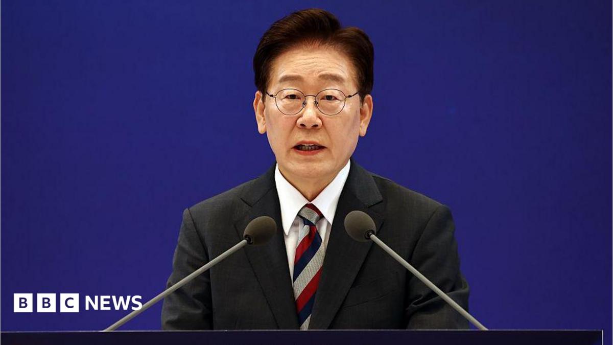
A $1 trillion state-backed investment will reshape the global AI hardware landscape and supply chain dynamics.
30-Second TL;DR
What Changed
Government-led $1 trillion investment initiative for AI and chip manufacturing.
Why It Matters
This massive capital injection will likely accelerate the global supply chain for AI hardware, potentially lowering costs for high-end compute resources. It signals a shift toward state-backed AI sovereignty in East Asia.
What To Do Next
Monitor South Korean semiconductor suppliers and AI hardware startups for potential partnership or supply chain opportunities.
Key Points
- •Government-led $1 trillion investment initiative for AI and chip manufacturing.
- •Strategic focus on maintaining competitiveness against Taiwan, China, and Japan.
- •Emphasis on expanding domestic chip factory capacity and AI technology development.
Deep Insight
AI-generated analysis for this event — not the original article.
Enhanced Key Takeaways
- •The investment initiative, often referred to as the 'K-Semiconductor Strategy,' includes significant tax credits and infrastructure support for private firms like Samsung Electronics and SK Hynix.
- •A core component of the funding is dedicated to the creation of a 'Mega Cluster' in Gyeonggi Province, designed to be the world's largest semiconductor supply chain hub.
- •The strategy prioritizes the development of next-generation High Bandwidth Memory (HBM) and Processing-in-Memory (PIM) technologies to dominate the AI hardware market.
- •South Korea is establishing specialized AI semiconductor research centers to reduce reliance on foreign-designed AI chips and foster a domestic fabless ecosystem.
- •The government has integrated workforce development programs into the plan, aiming to train over 30,000 specialized semiconductor engineers by 2030 to address critical talent shortages.
Competitor Analysis
- South Korea (K-Semiconductor)
- Memory & Logic Integration
- Taiwan (TSMC/Gov)
- Advanced Foundry (Logic)
- China (Big Fund)
- Self-Sufficiency/Legacy Nodes
- Japan (Rapidus/Gov)
- 2nm Logic & Packaging
- South Korea (K-Semiconductor)
- Mega Cluster/Tax Credits
- Taiwan (TSMC/Gov)
- Ecosystem/Subsidies
- China (Big Fund)
- State-Led Capital Injection
- Japan (Rapidus/Gov)
- Public-Private Consortium
- South Korea (K-Semiconductor)
- HBM Market Leadership
- Taiwan (TSMC/Gov)
- 3nm/2nm Foundry Dominance
- China (Big Fund)
- Massive Scale/Domestic Market
- Japan (Rapidus/Gov)
- Materials & Equipment Supply
| Feature | South Korea (K-Semiconductor) | Taiwan (TSMC/Gov) | China (Big Fund) | Japan (Rapidus/Gov) |
|---|---|---|---|---|
| Primary Focus | Memory & Logic Integration | Advanced Foundry (Logic) | Self-Sufficiency/Legacy Nodes | 2nm Logic & Packaging |
| Strategy | Mega Cluster/Tax Credits | Ecosystem/Subsidies | State-Led Capital Injection | Public-Private Consortium |
| Key Strength | HBM Market Leadership | 3nm/2nm Foundry Dominance | Massive Scale/Domestic Market | Materials & Equipment Supply |
Technical Deep Dive
- Focus on HBM4 and HBM4E development to support high-performance AI training clusters.
- Implementation of advanced packaging technologies including 3D IC and Chiplet architectures to improve power efficiency.
- Development of NPU (Neural Processing Unit) designs optimized for edge AI and large language model inference.
- Transition to Gate-All-Around (GAA) transistor architecture for sub-3nm logic manufacturing processes.
Future ImplicationsAI analysis grounded in cited sources
Timeline
- 2021-05South Korea announces the initial K-Semiconductor Strategy to secure global supply chain leadership.
- 2023-03Government unveils plans for the world's largest semiconductor mega-cluster in Yongin.
- 2024-01President Yoon Suk Yeol pledges expanded tax incentives for semiconductor R&D and facility investment.
- 2025-05South Korea formalizes the $1 trillion long-term investment framework to integrate AI and chip manufacturing.
Event Coverage
Weekly AI Recap
Read this week's curated digest of top AI events →
Related Updates

AI-curated news aggregator. All content rights belong to original publishers.
Original source: BBC Technology ↗
This is a summary, not the original. Read the source, or get the weekly briefing.
The weekly digest
One email a week. Unsubscribe anytime.