South Korea Invests $880B in AI Infrastructure
💡Massive $880B investment in AI infrastructure will reshape global chip supply chains.
⚡ 30-Second TL;DR
What Changed
Total investment target of $880 billion
Why It Matters
This massive capital injection will likely accelerate the supply of HBM and AI-ready chips, impacting global AI development timelines.
What To Do Next
Monitor the production capacity of HBM3e chips from Samsung and SK Hynix to forecast hardware availability for your AI clusters.
🧠 Deep Insight
AI-generated analysis for this event.
🔑 Enhanced Key Takeaways
- •The investment initiative is part of South Korea's 'AI Semiconductor Strategy,' which aims to capture a 10% share of the global AI chip market by 2030.
- •Government funding is specifically earmarked for the creation of an 'AI Semiconductor Innovation Center' to foster R&D collaboration between startups and conglomerates.
- •A significant portion of the capital is allocated to the development of High Bandwidth Memory (HBM) technologies, essential for training large-scale generative AI models.
- •The strategy includes tax incentives and deregulation measures designed to lower the barrier to entry for domestic fabless semiconductor companies.
- •South Korea is prioritizing the development of a sovereign AI cloud infrastructure to reduce reliance on foreign hyperscalers for national data processing.
📊 Competitor Analysis▸ Show
| Feature/Region | South Korea (AI Strategy) | United States (CHIPS Act) | European Union (EU Chips Act) |
|---|---|---|---|
| Primary Focus | HBM & Memory-Centric AI | Logic/GPU & Advanced Nodes | Automotive & Industrial Chips |
| Investment Scale | ~$880B (Total Ecosystem) | ~$52.7B (Direct Subsidies) | ~€43B (Public/Private) |
| Strategic Goal | Memory Dominance | Supply Chain Resiliency | Sovereignty & Manufacturing |
| Key Players | Samsung, SK Hynix | NVIDIA, Intel, AMD | Infineon, STMicroelectronics |
🛠️ Technical Deep Dive
- Focus on HBM4 and HBM4E memory architecture integration with logic chips to minimize data bottlenecks in AI training clusters.
- Implementation of Processing-in-Memory (PIM) technology to reduce power consumption by offloading data-intensive tasks directly to memory modules.
- Development of specialized AI accelerators (NPU) optimized for low-latency inference in edge computing environments.
- Integration of advanced packaging techniques such as 2.5D and 3D stacking (e.g., Samsung's I-Cube and H-Cube) to enhance chiplet interconnect density.
🔮 Future ImplicationsAI analysis grounded in cited sources
⏳ Timeline
Weekly AI Recap
Read this week's curated digest of top AI events →
👉Related Updates
Same topic
Explore #semiconductors
Same product
More on south-korea-ai-infrastructure
Same source
Latest from Bloomberg Technology

Anti-Data-Center Movement Impacts Michigan Political Landscape
Google Cloud Adds Specialist AI for Scientific Research
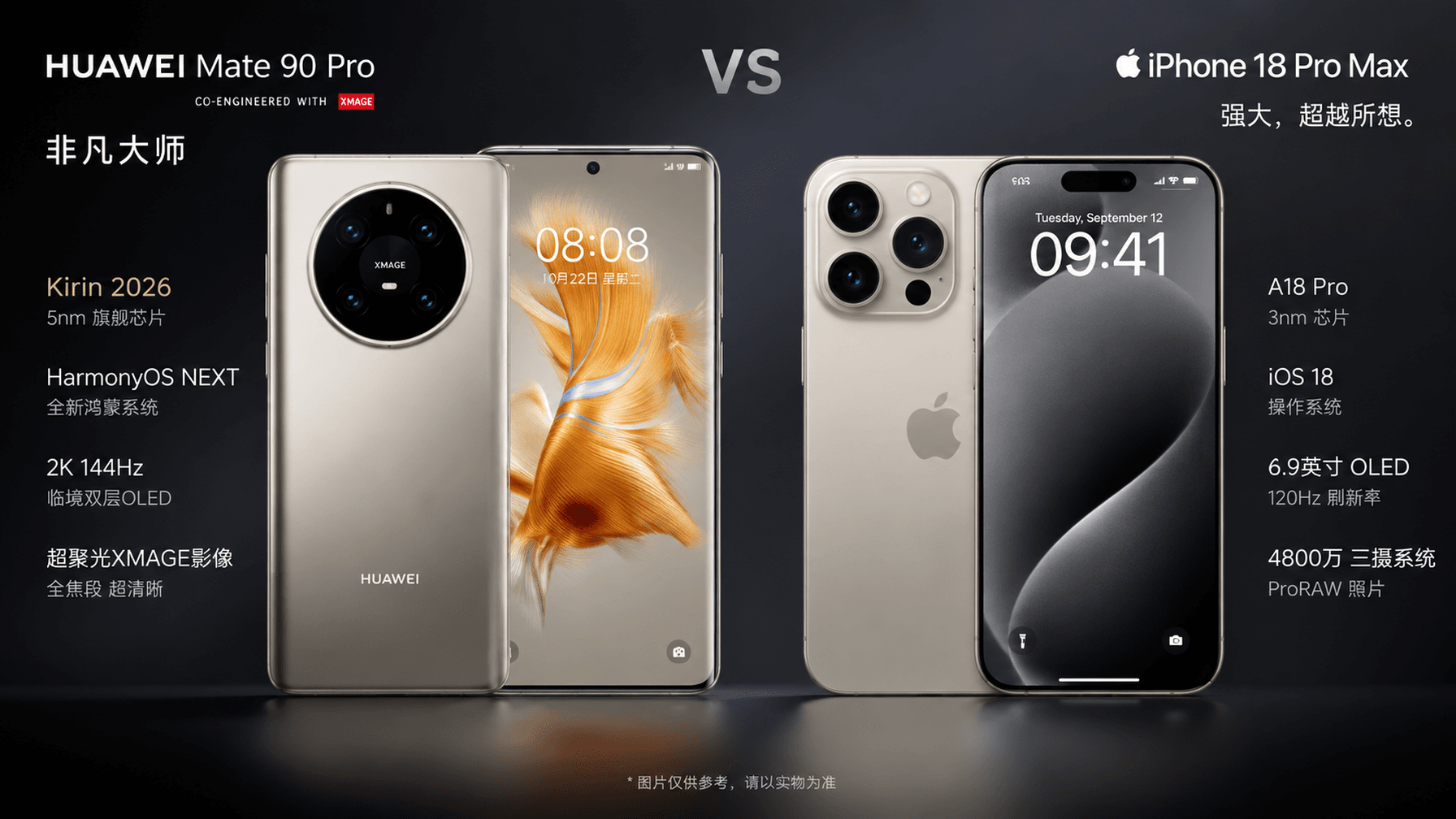
Huawei Mate 90 Launching September with Kirin 2026 Chip

Prosus profits double on e-commerce growth and Tencent stake
AI-curated news aggregator. All content rights belong to original publishers.
Original source: Bloomberg Technology ↗