Intel's Apple chip orders insufficient to challenge TSMC
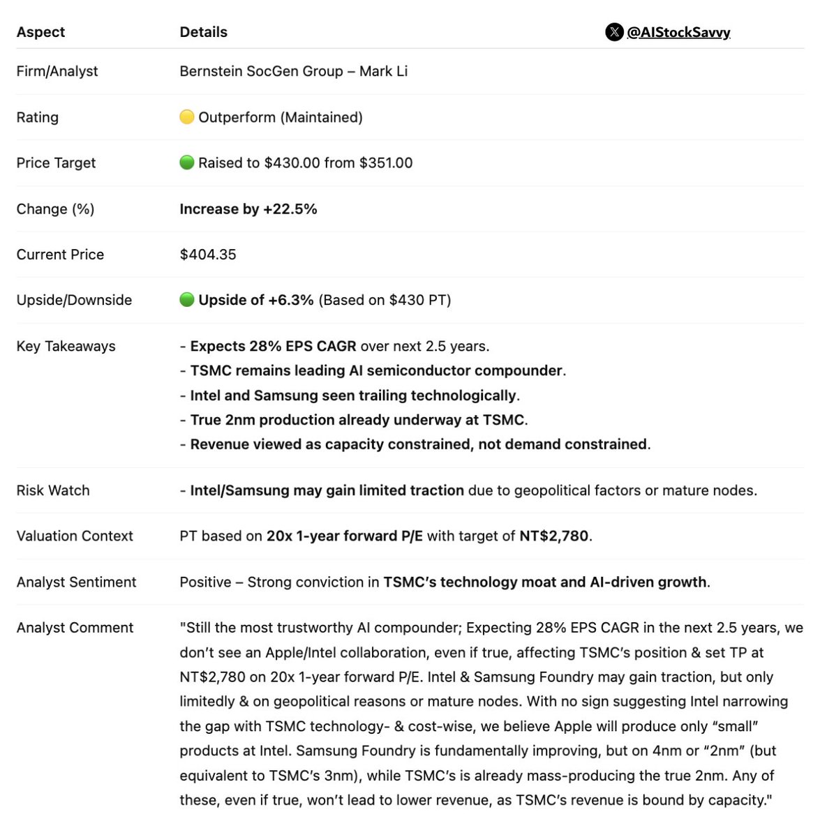
Understand the competitive landscape of AI chip manufacturing and TSMC's dominance in the supply chain.
30-Second TL;DR
What Changed
Bernstein report suggests Intel's Apple order volume is limited
Why It Matters
This confirms that TSMC's infrastructure and process node superiority in AI-capable silicon remains unchallenged by Intel's current foundry roadmap.
What To Do Next
Monitor TSMC's quarterly earnings and capacity expansion reports to gauge future AI hardware supply chain stability.
Key Points
- •Bernstein report suggests Intel's Apple order volume is limited
- •TSMC maintains its position as the leading AI chip manufacturer
- •Apple's diversification strategy does not signal a shift away from TSMC
Deep Insight
Background and context from public sources — not the original article. 34 sources cited.
Enhanced Key Takeaways
- •Apple's strategy to diversify its chip manufacturing partners, including Intel, is driven by a desire to enhance supply chain resilience, mitigate geopolitical risks associated with Taiwan, and address capacity constraints at TSMC due to surging AI demand.
- •Intel's 18A process node, a 2nm-class technology featuring RibbonFET (Gate-All-Around) transistors and PowerVia back-side power delivery, reached high-volume manufacturing (HVM) status in January 2026, offering significant performance and density improvements over previous Intel nodes.
- •Apple is reportedly evaluating Intel's 18A-P process for its lower-end M-series and A-series chips, with small-scale testing already underway and potential production ramping up in 2027 for entry-level MacBook Air, iPad models, and some iPhone chips.
- •The U.S. government has actively encouraged and potentially brokered the partnership between Apple and Intel, aligning with national security interests to expand domestic chip supply and reduce dependency on overseas manufacturing.
- •Despite potential orders from Apple, Bernstein analysts suggest that Intel is not narrowing the technology or cost gap with TSMC, which is already mass-producing true 2-nanometer chips and maintains a clear lead in advanced manufacturing.
Competitor Analysis
- TSMC
- ~70% (global, commanding majority)
- Intel Foundry Services (IFS)
- <1% (Q3 2024)
- Samsung Foundry
- 9.3% (Q3 2024)
- TSMC
- N3 (3nm), N2 (2nm in 2025)
- Intel Foundry Services (IFS)
- 18A (2nm-class, HVM Jan 2026)
- Samsung Foundry
- 3GAA (3nm, mid-2022)
- TSMC
- FinFET (N3), GAA nanosheet (N2 onwards)
- Intel Foundry Services (IFS)
- RibbonFET (GAA)
- Samsung Foundry
- MBCFET (GAA)
- TSMC
- CoWoS (critical for AI chips)
- Intel Foundry Services (IFS)
- EMIB, Foveros (3D packaging)
- Samsung Foundry
- (Not explicitly detailed in search results for comparison)
- TSMC
- Nvidia, Apple, Broadcom, Qualcomm
- Intel Foundry Services (IFS)
- Qualcomm, Amazon, Microsoft, (potential Apple for specific chips)
- Samsung Foundry
- (Not explicitly detailed in search results for comparison)
- TSMC
- Pure-play foundry, process leadership, AI/HPC
- Intel Foundry Services (IFS)
- Rebuilding process leadership, U.S. domestic supply, advanced packaging
- Samsung Foundry
- (Generally aims for advanced node competition and diversification)
| Feature/Company | TSMC | Intel Foundry Services (IFS) | Samsung Foundry |
|---|---|---|---|
| Market Share (Foundry) | ~70% (global, commanding majority) | <1% (Q3 2024) | 9.3% (Q3 2024) |
| Leading Process Node (HVM) | N3 (3nm), N2 (2nm in 2025) | 18A (2nm-class, HVM Jan 2026) | 3GAA (3nm, mid-2022) |
| Transistor Technology | FinFET (N3), GAA nanosheet (N2 onwards) | RibbonFET (GAA) | MBCFET (GAA) |
| Advanced Packaging | CoWoS (critical for AI chips) | EMIB, Foveros (3D packaging) | (Not explicitly detailed in search results for comparison) |
| Key Customers | Nvidia, Apple, Broadcom, Qualcomm | Qualcomm, Amazon, Microsoft, (potential Apple for specific chips) | (Not explicitly detailed in search results for comparison) |
| Strategic Focus | Pure-play foundry, process leadership, AI/HPC | Rebuilding process leadership, U.S. domestic supply, advanced packaging | (Generally aims for advanced node competition and diversification) |
Technical Deep Dive
- Intel 18A Process:
- A 2nm-class node, representing a significant leap in Intel's process technology.
- Features RibbonFET (Gate-All-Around, GAA) transistors, which replace the traditional FinFET design, offering superior control over electrical leakage and higher drive currents.
- Incorporates PowerVia back-side power delivery, which moves power routing to the backside of the die, freeing up front-side space for more efficient signal routing and reduced congestion.
- Delivers up to 15% better performance per watt and up to 30% better chip density compared to the Intel 3 process node.
- Reached high-volume manufacturing (HVM) status in January 2026.
- TSMC N3/N2 Process:
- N3 (3nm): Offers a 10-15% increase in performance or a 25-35% decrease in power consumption, with a 70% increase in logic density compared to its N5 process. This node still utilizes FinFET technology.
- N3E: An optimized version of the 3nm node, providing approximately a 20% speed improvement, over 30% power savings, and about 1.6 times logic density increase compared to N5 technology.
- N2 (2nm): Expected to enter volume production in 2025, N2 will be TSMC's first node to adopt Gate-All-Around (GAA) nanosheet transistors, marking a transition from FinFET.
- N2 is projected to offer 25-30% power reductions at the same speed, or a 10-15% performance boost at the same power, with chip densities increasing by 1.15x or more compared to N3E.
- TSMC's next-generation A16 technology is also expected to see significant capacity growth between 2026 and 2028.
- Advanced Packaging: Both Intel (with EMIB and Foveros) and TSMC (with CoWoS) are heavily investing in advanced 3D packaging solutions, which are crucial for integrating multiple chiplets and high-bandwidth memory in high-performance AI accelerators.
Future ImplicationsAI analysis grounded in cited sources
Timeline
- 2010Apple intensified its search for a manufacturing partner beyond Samsung, initiating discussions with TSMC.
- 2013TSMC made a significant $10 billion investment in 20nm capacity, with Apple as a promised key customer.
- 2014Apple's A8 chip, manufactured by TSMC, launched, marking a pivotal moment in their partnership.
- 2016TSMC became the exclusive supplier of Apple's systems-on-a-chip (SoCs) for its mobile devices.
- 2021Intel established its Foundry Services (IFS) arm with a $20 billion investment, aiming to produce chips designed by other companies.
- 2026-01Intel's 18A process node reached high-volume manufacturing (HVM) status.
- 2026-05Reports indicate Apple is evaluating Intel's 18A-P process for lower-end M-series and A-series chips, with potential production starting in 2027.
Sources (34)
Factual claims are grounded in the sources below. Forward-looking analysis is AI-generated interpretation.
Weekly AI Recap
Read this week's curated digest of top AI events →
Related Updates

AI-curated news aggregator. All content rights belong to original publishers.
Original source: cnBeta (Full RSS) ↗
This is a summary, not the original. Read the source, or get the weekly briefing.
The weekly digest
One email a week. Unsubscribe anytime.