📱Engadget•Freshcollected in 21m
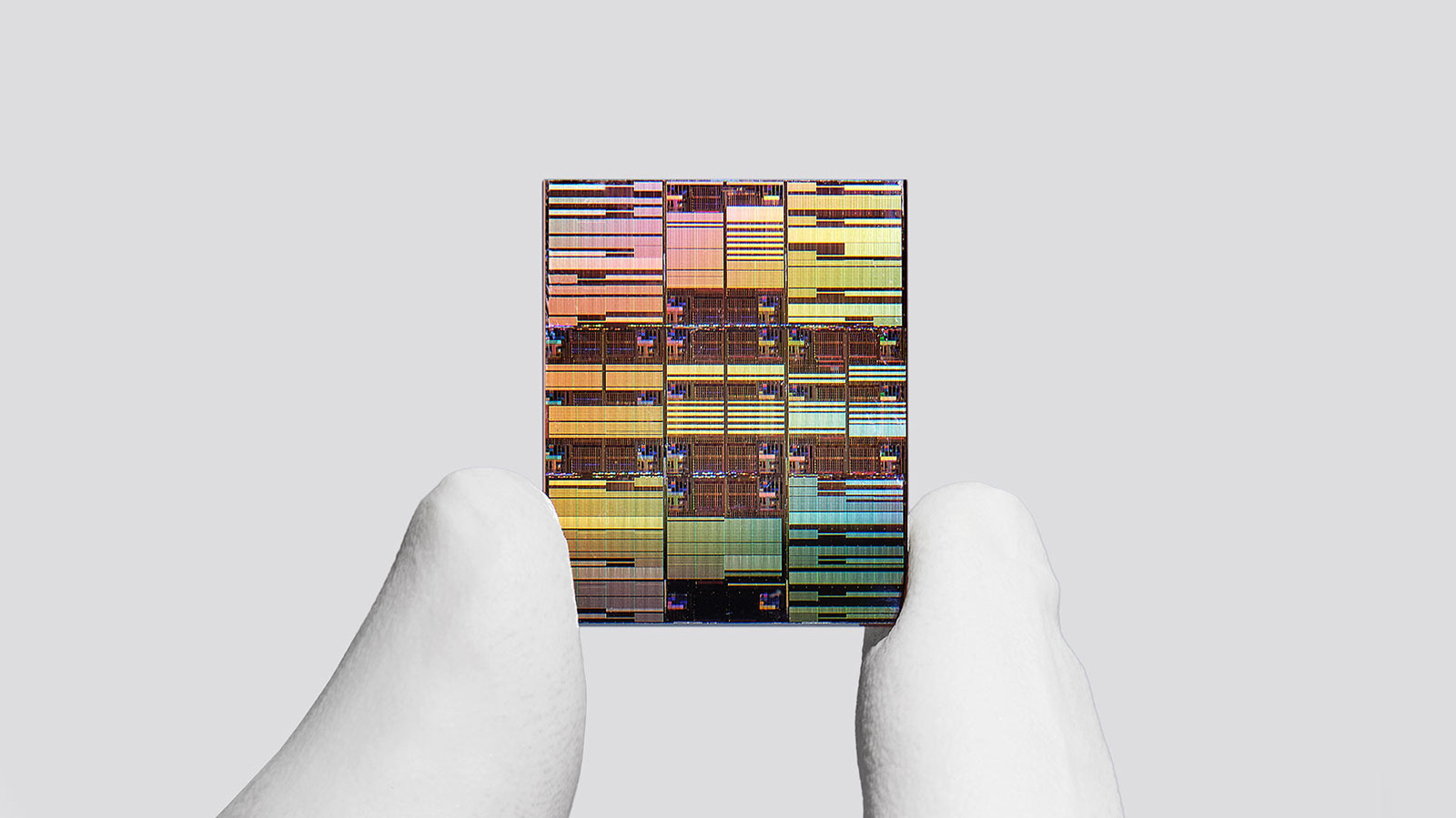
IBM Unveils World's First Sub-1nm Chip Technology
💡Sub-1nm chips are the future of AI compute; this is the hardware foundation for the next decade of AI.
⚡ 30-Second TL;DR
What Changed
First successful demonstration of sub-1nm chip architecture
Why It Matters
This breakthrough is critical for the future of AI infrastructure, as it allows for more powerful, energy-efficient chips required for large-scale model training.
What To Do Next
Monitor IBM's research publications to understand the timeline for commercial availability of sub-1nm nodes for AI accelerators.
Who should care:Researchers & Academics
🧠 Deep Insight
AI-generated analysis for this event.
🔑 Enhanced Key Takeaways
- •The breakthrough utilizes nanosheet transistor architecture, evolving beyond the FinFET designs used in previous generations.
- •IBM's process integrates a new gate-all-around (GAA) methodology to maintain electrostatic control at sub-1nm dimensions.
- •The technology incorporates proprietary backside power delivery networks to mitigate voltage droop and improve signal integrity.
- •Research indicates the use of novel 2D materials, such as molybdenum disulfide, to replace traditional silicon channels at these scales.
- •The manufacturing process leverages extreme ultraviolet (EUV) lithography with high-numerical aperture (High-NA) optics to achieve the required resolution.
📊 Competitor Analysis▸ Show
| Feature | IBM (Sub-1nm) | TSMC (2nm/1.4nm) | Intel (14A/10A) |
|---|---|---|---|
| Architecture | GAA Nanosheet | GAA (Nanosheet) | RibbonFET (GAA) |
| Status | Research/Prototype | Production/Pilot | Development |
| Primary Focus | High-Performance AI | Foundational Scaling | Power Efficiency |
🛠️ Technical Deep Dive
- Architecture: Utilizes stacked nanosheet transistors to maximize current drive per unit area.
- Channel Material: Transition from bulk silicon to 2D transition metal dichalcogenides (TMDs) to suppress short-channel effects.
- Interconnects: Employs ruthenium-based metallization to reduce resistance at atomic scales where copper suffers from electron scattering.
- Power Delivery: Backside power delivery network (BSPDN) separates signal and power routing to reduce parasitic capacitance.
🔮 Future ImplicationsAI analysis grounded in cited sources
AI model training energy consumption will decrease by at least 40% per operation.
The increased transistor density and reduced parasitic capacitance allow for lower operating voltages while maintaining high switching speeds.
Commercial availability of sub-1nm chips will not occur before 2029.
Current industry roadmaps for high-volume manufacturing (HVM) indicate that 1.4nm and 1nm nodes are scheduled for late-decade production, with sub-1nm requiring further yield stabilization.
⏳ Timeline
2017-06
IBM demonstrates the industry's first 5nm silicon nanosheet transistor.
2021-05
IBM unveils the world's first 2nm chip technology.
2023-04
IBM and partners announce breakthroughs in 2nm nanosheet yield and performance.
2026-06
IBM announces the world's first sub-1nm chip technology demonstration.
📰 Event Coverage
📰
Weekly AI Recap
Read this week's curated digest of top AI events →
👉Related Updates


AI-curated news aggregator. All content rights belong to original publishers.
Original source: Engadget ↗