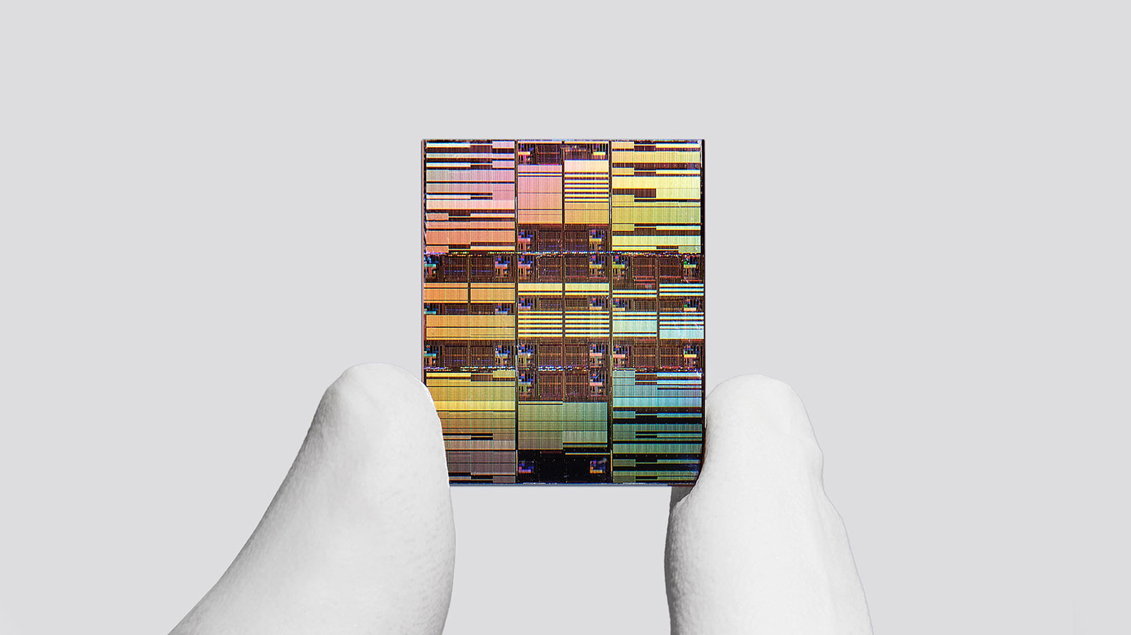
IBM Unveils World's First Sub-1 Nanometer Chip Technology
💡Sub-1nm chips are the next frontier for AI hardware, promising massive gains in compute efficiency and power density.
⚡ 30-Second TL;DR
What Changed
IBM successfully developed the world's first sub-1nm chip technology.
Why It Matters
This breakthrough could lead to a new generation of AI-optimized hardware, reducing power consumption for massive model training and inference. It reinforces the critical role of physical infrastructure in sustaining the current AI development pace.
What To Do Next
Monitor IBM's research roadmap for potential partnerships or cloud availability of these high-density chips for future AI model training.
🧠 Deep Insight
AI-generated analysis for this event.
🔑 Enhanced Key Takeaways
- •The technology utilizes nanosheet transistor architecture, an evolution of the Gate-All-Around (GAA) design previously pioneered by IBM in 2021.
- •IBM is leveraging high-NA EUV (Extreme Ultraviolet) lithography tools to achieve the precision required for sub-1nm feature sizes.
- •The breakthrough incorporates new materials beyond traditional silicon, specifically utilizing 2D semiconductor materials like molybdenum disulfide to maintain electron mobility at such small scales.
- •This manufacturing process addresses quantum tunneling issues, a primary physical barrier that typically causes leakage current in transistors below the 2nm threshold.
- •IBM is collaborating with partners in the Albany NanoTech Complex to transition this laboratory-scale success into a viable high-volume manufacturing (HVM) process.
📊 Competitor Analysis▸ Show
| Feature | IBM (Sub-1nm) | TSMC (2nm/A16) | Intel (14A/10A) |
|---|---|---|---|
| Architecture | Nanosheet / 2D Materials | Nanosheet (GAA) | RibbonFET (GAA) |
| Status | Research Breakthrough | HVM Expected 2025/2026 | HVM Expected 2026/2027 |
| Primary Focus | R&D / IP Licensing | Foundry / High Volume | Foundry / Internal Compute |
🛠️ Technical Deep Dive
- Utilizes 2D transition metal dichalcogenides (TMDs) to overcome the short-channel effects inherent in silicon at sub-1nm dimensions.
- Employs a stacked nanosheet configuration to maximize effective channel width within a minimal footprint.
- Integrates backside power delivery networks (BSPDN) to reduce IR drop and improve signal integrity for high-frequency AI workloads.
- Utilizes atomic layer deposition (ALD) to achieve sub-angstrom precision in layer thickness control.
🔮 Future ImplicationsAI analysis grounded in cited sources
⏳ Timeline
Weekly AI Recap
Read this week's curated digest of top AI events →
👉Related Updates
Same topic
Explore #semiconductor
Same product
More on ibm-sub-1nm-chip-technology
Same source
Latest from Bloomberg Technology
IBM Unveils World's First Sub-1nm Chip Technology
Cerebras Shares Tumble Following Disappointing Sales Outlook
AI Transforms Memory into Strategic Semiconductor Asset
Apple Pivots to AI-Focused M7 Mac Silicon
AI-curated news aggregator. All content rights belong to original publishers.
Original source: Bloomberg Technology ↗