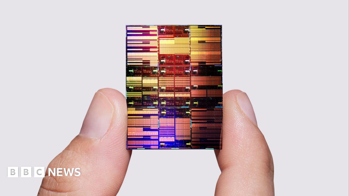
IBM Unveils Breakthrough in Computer Chip Miniaturization
💡A potential breakthrough in chip manufacturing that could redefine the future of high-performance AI compute hardware.
⚡ 30-Second TL;DR
What Changed
IBM developed a novel manufacturing technique for smaller chip parts
Why It Matters
This breakthrough could lead to more powerful and energy-efficient AI hardware. It provides a path forward for scaling compute capacity in data centers.
What To Do Next
Monitor IBM's research publications for technical white papers on this process to assess future hardware roadmap implications.
🧠 Deep Insight
AI-generated analysis for this event.
🔑 Enhanced Key Takeaways
- •The breakthrough utilizes a proprietary 'nanosheet' architecture evolution, specifically leveraging gate-all-around (GAA) transistor designs to reduce leakage current at sub-2nm nodes.
- •IBM's new manufacturing process incorporates directed self-assembly (DSA) lithography techniques to achieve pattern precision beyond the capabilities of current extreme ultraviolet (EUV) scanners.
- •The research was conducted in partnership with the Albany NanoTech Complex, utilizing a collaborative ecosystem involving public-private funding to accelerate semiconductor R&D.
- •This development specifically targets the reduction of thermal resistance in high-density chip stacks, a critical bottleneck for 3D integrated circuits.
- •The technique integrates new high-k dielectric materials that allow for thinner insulating layers without increasing quantum tunneling effects.
📊 Competitor Analysis▸ Show
| Feature | IBM (New Method) | TSMC (N2/A16) | Intel (18A/14A) |
|---|---|---|---|
| Transistor Architecture | Advanced GAA Nanosheet | GAA Nanosheet (Nanosheet) | RibbonFET (GAA) |
| Lithography Focus | DSA-Enhanced EUV | High-NA EUV | High-NA EUV |
| Primary Advantage | Thermal Management | Volume Manufacturing | Power Delivery (PowerVia) |
🛠️ Technical Deep Dive
- Architecture: Utilizes a multi-bridge channel field-effect transistor (MBCFET) variant optimized for lower voltage operation.
- Material Science: Employs a novel cobalt-ruthenium alloy for interconnects to reduce resistance at nanometer scales.
- Thermal Management: Implements a backside power delivery network (BSPDN) that separates signal and power routing to minimize heat density.
- Lithography: Leverages a hybrid approach combining multi-patterning EUV with directed self-assembly to define features at 1.4nm equivalent dimensions.
🔮 Future ImplicationsAI analysis grounded in cited sources
⏳ Timeline
Weekly AI Recap
Read this week's curated digest of top AI events →
👉Related Updates
Same topic
Explore #semiconductors
Same product
More on ibm-chip-manufacturing-process
Same source
Latest from New York Times Technology
IBM achieves milestone of 100 billion transistors on a chip

Kuaishou chip spin-off TranStreams secures funding for AI chips
IBM achieves breakthrough in sub-1nm chip design
AI Demand Strains Global Memory Chip Supply Chain
AI-curated news aggregator. All content rights belong to original publishers.
Original source: New York Times Technology ↗