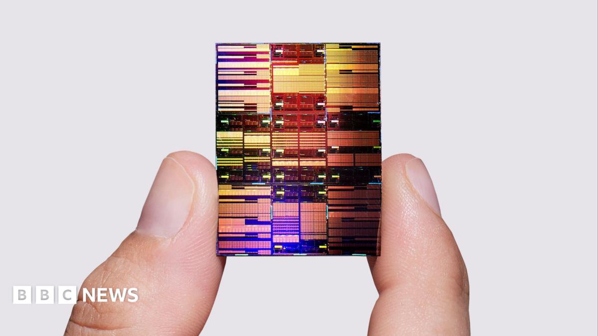
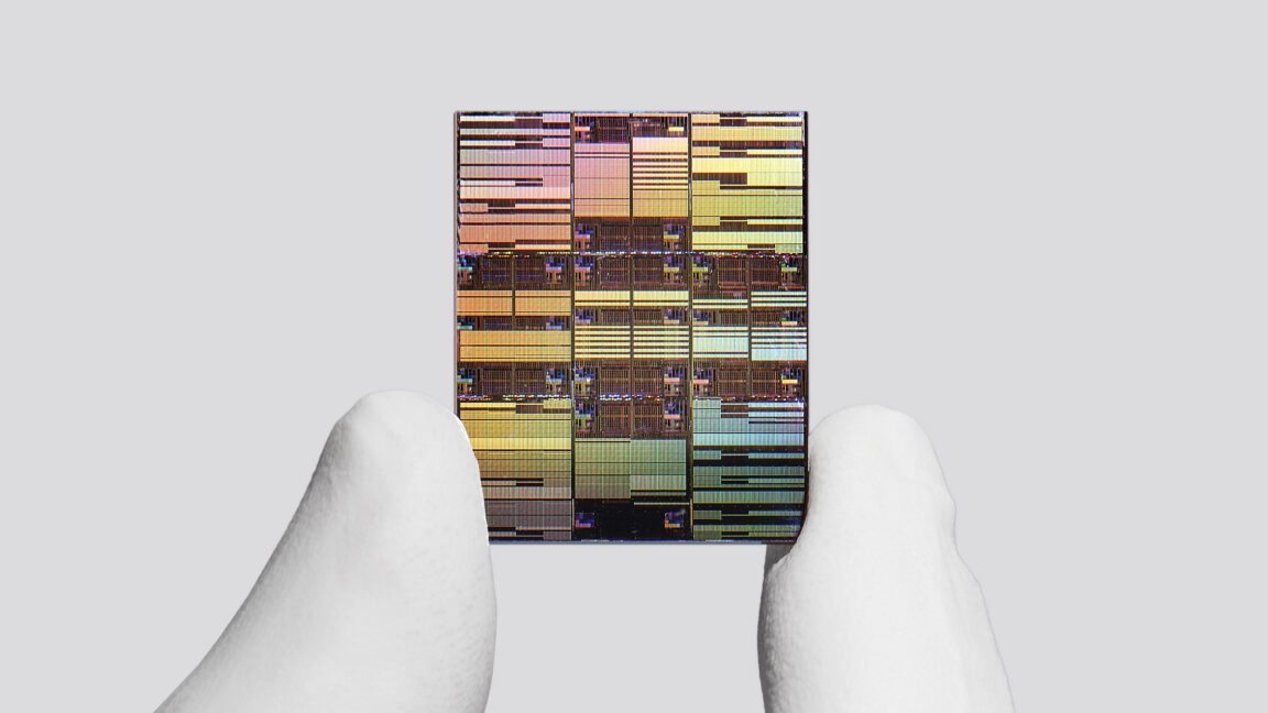
IBM achieves breakthrough in sub-1nm chip design
💡Sub-1nm chips are the future of AI compute; understand the architectural shifts that will power next-gen AI hardware.
⚡ 30-Second TL;DR
What Changed
IBM developed a 'block of flats' vertical stacking architecture for transistors.
Why It Matters
This advancement could eventually lead to significantly more powerful and energy-efficient AI hardware, potentially overcoming current scaling limits in GPU and NPU development.
What To Do Next
Monitor IBM's research publications for updates on thermal management and power efficiency metrics for sub-1nm architectures.
🧠 Deep Insight
AI-generated analysis for this event.
🔑 Enhanced Key Takeaways
- •The 'block of flats' architecture refers to Complementary Field-Effect Transistor (CFET) technology, which allows n-type and p-type transistors to be stacked vertically rather than placed side-by-side.
- •This design utilizes nanosheet transistor technology, an evolution from the FinFET architecture that has dominated semiconductor manufacturing for the past decade.
- •IBM's research utilizes Extreme Ultraviolet (EUV) lithography, specifically leveraging high-numerical aperture (High-NA) EUV tools to achieve the precision required for sub-1nm features.
- •The breakthrough addresses the 'short-channel effect'—a common issue in shrinking transistors where gate control over the current flow diminishes as dimensions decrease.
- •IBM is collaborating with partners in the Albany NanoTech Complex to refine the material science required to prevent quantum tunneling, which typically destabilizes transistors at these scales.
📊 Competitor Analysis▸ Show
| Feature | IBM (CFET/Nanosheet) | TSMC (Nanosheet/GAA) | Intel (RibbonFET/GAA) |
|---|---|---|---|
| Architecture | Vertical CFET | Gate-All-Around (GAA) | Gate-All-Around (GAA) |
| Status | Research/Prototype | Production (2nm) | Production (20A/18A) |
| Focus | Density/Power Efficiency | High-Volume Manufacturing | Performance/Power Scaling |
🛠️ Technical Deep Dive
- Architecture: Complementary FET (CFET) design enabling 3D stacking of nFET and pFET devices.
- Transistor Type: Gate-All-Around (GAA) Nanosheets providing superior electrostatic control compared to traditional FinFETs.
- Lithography: High-NA EUV (0.55 NA) required for patterning sub-1nm critical dimensions.
- Material Science: Integration of high-k metal gates and advanced channel materials to mitigate leakage currents at atomic scales.
- Interconnects: Utilization of backside power delivery networks to reduce resistance and improve signal integrity in dense layouts.
🔮 Future ImplicationsAI analysis grounded in cited sources
⏳ Timeline
Weekly AI Recap
Read this week's curated digest of top AI events →
👉Related Updates
Same topic
Explore #semiconductors
Same product
More on ibm-sub-1nm-chip-technology
Same source
Latest from BBC Technology

Kuaishou chip spin-off TranStreams secures funding for AI chips
IBM unveils world's first sub-1 nanometer chip technology
IBM achieves milestone of 100 billion transistors on a chip
IBM Unveils Breakthrough in Computer Chip Miniaturization
AI-curated news aggregator. All content rights belong to original publishers.
Original source: BBC Technology ↗