CXMT IPO Approved for DRAM Technology Expansion
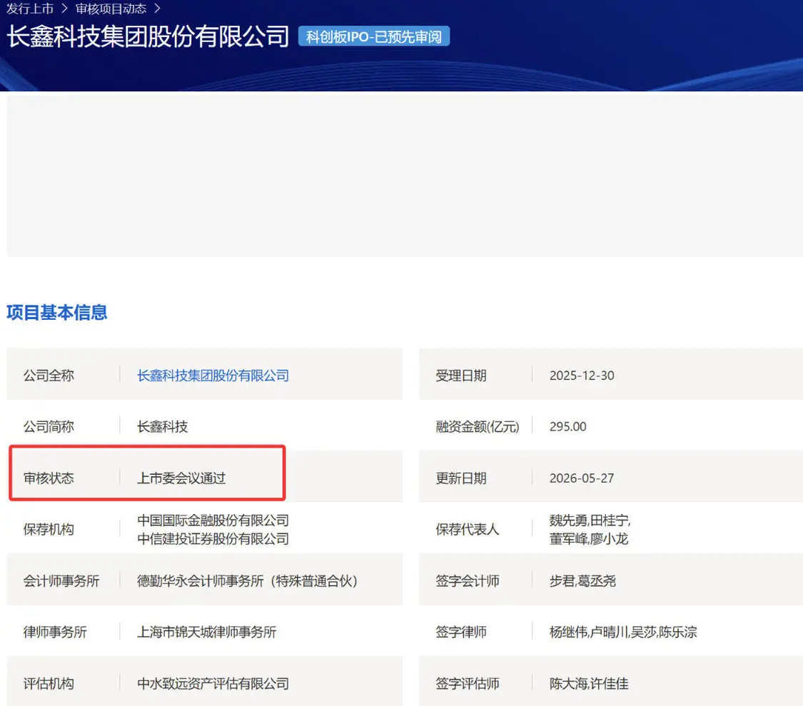
Major funding for domestic DRAM production, critical for AI hardware supply chains in China.
30-Second TL;DR
What Changed
IPO approval for 29.5 billion RMB fundraising on STAR Market
Why It Matters
This massive capital injection will accelerate China's domestic DRAM production capabilities, potentially easing supply constraints for local AI hardware manufacturers.
What To Do Next
Monitor CXMT's supply chain availability if you are building local AI server infrastructure in China.
Key Points
- •IPO approval for 29.5 billion RMB fundraising on STAR Market
- •Focus on DRAM manufacturing line upgrades and capacity expansion
- •Investment in advanced DRAM R&D for future memory technologies
Deep Insight
Background and context from public sources — not the original article. 18 sources cited.
Enhanced Key Takeaways
- •CXMT's IPO aims to raise approximately 29.5 billion RMB (around $4.2 billion to $4.3 billion USD), with the potential to exceed $5 billion if an over-allotment option is exercised, positioning it as one of China's largest semiconductor listings.
- •The company demonstrated significant financial growth in Q1 2026, reporting a year-over-year revenue surge exceeding 700% and a net profit increase of 1,688%, largely attributed to a global rise in memory chip demand driven by AI infrastructure.
- •As of Q4 2025/Q1 2026, CXMT has secured a global DRAM market share of approximately 7.67% to 8%, establishing itself as the world's fourth-largest DRAM producer, behind Samsung, SK Hynix, and Micron.
- •Beyond current manufacturing, CXMT is actively developing High Bandwidth Memory (HBM), including HBM3 in collaboration with Huawei, and plans to expand production of its DDR4 and LPDDR5/5X chips.
- •The IPO application process, initially filed in December 2025, experienced a temporary halt in early 2026 due to expired financial documents before resuming in May 2026, culminating in approval on May 27, 2026.
Competitor Analysis
- CXMT
- ~8%
- Samsung Electronics
- 38%
- SK Hynix
- 29%
- Micron Technology
- 22%
- CXMT
- 16Gb/24Gb
- Samsung Electronics
- Up to 32Gb (leading edge)
- SK Hynix
- Up to 32Gb (leading edge)
- Micron Technology
- Up to 32Gb (leading edge)
- CXMT
- 16.0 nm (G4 DRAM, D1z equivalent)
- Samsung Electronics
- 12-14 nm (D1a/D1α, D1b/D1β)
- SK Hynix
- 12-14 nm (D1a/D1α, D1b/D1β)
- Micron Technology
- 12-14 nm (D1a/D1α, D1b/D1β)
- CXMT
- ~3 years behind leaders
- Samsung Electronics
- Leading edge
- SK Hynix
- Leading edge
- Micron Technology
- Leading edge
- CXMT
- HBM3 (with Huawei)
- Samsung Electronics
- HBM4 (leading)
- SK Hynix
- HBM4 (leading, secured Nvidia orders)
- Micron Technology
- HBM4 (aggressively expanding)
- CXMT
700%
- Samsung Electronics
- Significant growth (reclaimed #1 DRAM revenue Q4 2025)
- SK Hynix
- Significant growth (58% operating profit margin Q4 2025)
- Micron Technology
- Record revenues (Q1 FY2026)
| Feature/Metric | CXMT | Samsung Electronics | SK Hynix | Micron Technology |
|---|---|---|---|---|
| Global DRAM Market Share (Q1 2026) | ~8% | 38% | 29% | 22% |
| Latest DDR5 Capacity | 16Gb/24Gb | Up to 32Gb (leading edge) | Up to 32Gb (leading edge) | Up to 32Gb (leading edge) |
| DRAM Process Node (DDR5) | 16.0 nm (G4 DRAM, D1z equivalent) | 12-14 nm (D1a/D1α, D1b/D1β) | 12-14 nm (D1a/D1α, D1b/D1β) | 12-14 nm (D1a/D1α, D1b/D1β) |
| Technology Gap (DDR5) | ~3 years behind leaders | Leading edge | Leading edge | Leading edge |
| HBM Development | HBM3 (with Huawei) | HBM4 (leading) | HBM4 (leading, secured Nvidia orders) | HBM4 (aggressively expanding) |
| Q1 2026 Revenue Growth (YoY) | 700% | Significant growth (reclaimed #1 DRAM revenue Q4 2025) | Significant growth (58% operating profit margin Q4 2025) | Record revenues (Q1 FY2026) |
Technical Deep Dive
- DRAM Generations: CXMT produces LPDDR4 and DDR4 memory, and has advanced to DDR5 and LPDDR5/5X.
- Process Technology: Initially used a 19 nm process (referred to as 10G1 process technology) for DDR4 and LPDDR4.
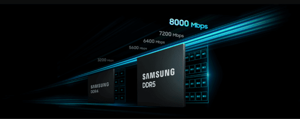
- DDR5 Specifications: CXMT's DDR5 chips feature 16Gb and 24Gb die capacities, achieving speeds up to 8000Mbps. They incorporate on-die ECC (Error Correction Code) and enhanced anti-interference designs.
- LPDDR5/5X Specifications: CXMT's LPDDR5X offers 12Gb/16Gb die capacity and speeds up to 10667Mbps, with a 30% power consumption reduction compared to LPDDR5.
- Feature Size (DDR5): The company's G4 DRAM generation for DDR5 uses a 16.0 nm feature size, which corresponds to the D1z generation. This represents a 20% reduction in cell size from their previous G3 (18.0 nm) DRAM node.
- Future R&D: CXMT is aggressively developing next-generation sub-15 nm technology without relying on EUV lithography, and is also focusing on High Bandwidth Memory (HBM), including HBM3 in collaboration with Huawei.
- Manufacturing Capacity: As of 2020, CXMT had a capacity of 40,000 wafers per month, which increased to 720,000 wafers per quarter by the end of 2025.
Future ImplicationsAI analysis grounded in cited sources
Timeline
- 2016CXMT (originally Innotron Memory) founded in Hefei, Anhui, with the goal of competing with global memory manufacturers.
- 2017A $7.2 billion deal for a 125,000, 12-inch wafer per month production fabrication plant was announced, with the factory completed mid-year and equipment installed late year.
- 2019-12CXMT became China's first domestic DRAM supplier, commencing production of LPDDR4 and DDR4 8Gbit chips using a 10-nanometer class (18 or 19 nm) node at 20,000 wafers per month.
- 2020LPDDR4 RAM was added to the product portfolio, and manufacturing capacity reached 40,000 wafers per month.
- 2025-01CXMT released its 16Gb DDR5 chips to the market, featuring a 16.0 nm feature size (G4 DRAM generation).
- 2025-12CXMT first submitted its IPO application to the Shanghai Stock Exchange under a newly introduced pre-review system.
- 2026-05-27The Shanghai Stock Exchange Listing Review Committee formally evaluated and approved CXMT's IPO application on the STAR Market.
Sources (18)
Factual claims are grounded in the sources below. Forward-looking analysis is AI-generated interpretation.
Weekly AI Recap
Read this week's curated digest of top AI events →
Related Updates

AI-curated news aggregator. All content rights belong to original publishers.
Original source: cnBeta (Full RSS) ↗
This is a summary, not the original. Read the source, or get the weekly briefing.
The weekly digest
One email a week. Unsubscribe anytime.