TSMC Glass Substrates: Essential for Next-Gen AI Chips
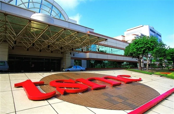
💡Glass substrates are the next bottleneck for AI compute; understand the hardware shift powering future GPU performance.
⚡ 30-Second TL;DR
What Changed
Glass core substrates are mandatory for next-gen AI chip performance
Why It Matters
This shift in packaging technology will likely define the next wave of AI hardware performance and power efficiency. Practitioners should monitor supply chain shifts as glass substrates become the new standard for high-end AI accelerators.
What To Do Next
Monitor hardware spec sheets for upcoming AI accelerators to see if they transition to glass-core packaging for improved thermal headroom.
Key Points
- •Glass core substrates are mandatory for next-gen AI chip performance
- •TSMC is partnering with Ibiden and Innolux for development
- •The design features a glass core sandwiched between two ABF layers
🧠 Deep Insight
AI-generated analysis for this event — not the original article.
🔑 Enhanced Key Takeaways
- •Glass substrates offer superior thermal stability and flatness compared to traditional organic substrates, which is critical for preventing warpage in large-die AI accelerators.
- •The transition to glass cores enables higher interconnect density, allowing for finer pitch routing that supports the increased I/O requirements of next-generation HBM (High Bandwidth Memory) integration.
- •Glass substrates possess a lower dielectric loss tangent, which significantly improves signal integrity for high-speed data transmission between chiplets in advanced packaging.
- •TSMC's adoption of glass substrates is part of a broader industry shift to overcome the physical limitations of ABF (Ajinomoto Build-up Film) substrates as chip sizes approach the reticle limit.
- •The collaboration with Ibiden and Innolux leverages Ibiden's expertise in high-end IC packaging and Innolux's existing glass panel manufacturing infrastructure to accelerate mass production readiness.
📊 Competitor Analysis▸ Show
| Feature | TSMC (Glass Core) | Intel (Glass Substrate) | Samsung (Glass Substrate) |
|---|---|---|---|
| Status | Pilot/Development | Advanced R&D | R&D/Pilot |
| Key Partner | Ibiden/Innolux | Internal/In-house | Samsung Electro-Mechanics |
| Focus | AI Accelerator Packaging | Data Center/Server CPUs | Mobile/AI SoC |
| Advantage | Ecosystem Integration | Early R&D Leadership | Vertical Integration |
🛠️ Technical Deep Dive
- Glass Core Structure: Utilizes a rigid glass panel as the central carrier, replacing the traditional organic resin core.
- Thermal Expansion: Glass provides a Coefficient of Thermal Expansion (CTE) that more closely matches silicon, reducing mechanical stress during thermal cycling.
- Interconnects: Employs Through-Glass Vias (TGV) to provide vertical electrical connections, offering better electrical performance than traditional Through-Mold Vias (TMV).
- Layering: The three-layer architecture consists of a central glass core with ABF layers applied to both sides to facilitate high-density copper wiring.
- Dimensional Stability: Glass exhibits significantly less shrinkage and expansion during the lamination process, enabling tighter alignment for multi-chiplet assemblies.
🔮 Future ImplicationsAI analysis grounded in cited sources
⏳ Timeline
Weekly AI Recap
Read this week's curated digest of top AI events →
👉Related Updates

AI-curated news aggregator. All content rights belong to original publishers.
Original source: cnBeta (Full RSS) ↗
This is a summary, not the original. Read the source, or get the weekly briefing.
Weekly AI briefing
One email a week. Unsubscribe anytime.