Sony Teams with TSMC on Image Sensors
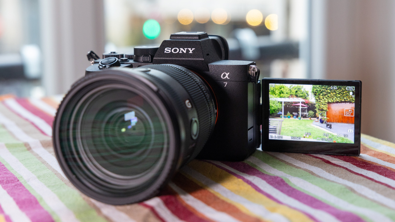
Sony-TSMC facility boosts image sensor supply critical for AI vision hardware.
30-Second TL;DR
What Changed
Sony seeks TSMC's help for image sensors
Why It Matters
Partnership could scale image sensor supply for AI vision systems in devices and robotics. May lower costs and improve availability for computer vision hardware.
What To Do Next
Monitor TSMC sensor yields for optimizing edge AI vision model deployments.
Key Points
- •Sony seeks TSMC's help for image sensors
- •Teaming up on new production facility
- •Focus on advanced sensor manufacturing
Deep Insight
AI-generated analysis for this event — not the original article.
Enhanced Key Takeaways
- •The partnership centers on the JASM (Japan Advanced Semiconductor Manufacturing) facility in Kumamoto, Japan, a joint venture between TSMC, Sony Semiconductor Solutions, and Denso.
- •The collaboration specifically targets the production of 22/28nm and 12/16nm FinFET process technologies to support the increasing demand for high-performance CMOS image sensors.
- •This strategic move is heavily supported by the Japanese government's subsidy program, which aims to revitalize domestic semiconductor manufacturing and secure supply chain resilience for critical imaging components.
Competitor Analysis
- Sony (JASM)
- CMOS Image Sensors (CIS)
- Samsung Foundry
- Logic + CIS
- Tower Semiconductor
- Specialized Analog/CIS
- Sony (JASM)
- 12nm - 28nm
- Samsung Foundry
- 5nm - 28nm
- Tower Semiconductor
- 65nm - 180nm
- Sony (JASM)
- Vertical Integration
- Samsung Foundry
- Foundational Competition
- Tower Semiconductor
- Niche/Automotive CIS
| Feature | Sony (JASM) | Samsung Foundry | Tower Semiconductor |
|---|---|---|---|
| Primary Focus | CMOS Image Sensors (CIS) | Logic + CIS | Specialized Analog/CIS |
| Process Nodes | 12nm - 28nm | 5nm - 28nm | 65nm - 180nm |
| Market Strategy | Vertical Integration | Foundational Competition | Niche/Automotive CIS |
Technical Deep Dive
- •Utilization of TSMC's 12/16nm FinFET process allows for higher logic density and lower power consumption compared to traditional planar processes used in older image sensor generations.
- •Integration of Sony's proprietary stacked CMOS image sensor architecture with TSMC's advanced logic wafers enables improved signal-to-noise ratios and faster readout speeds.
- •The manufacturing process involves wafer-to-wafer bonding technology, allowing the pixel array (manufactured by Sony) to be combined with the logic circuit (manufactured by TSMC) for optimized performance.
Future ImplicationsAI analysis grounded in cited sources
Timeline
- 2021-11Sony and TSMC announce the formation of JASM in Kumamoto, Japan.
- 2022-02Denso joins the JASM joint venture to strengthen automotive semiconductor supply.
- 2024-02JASM officially opens its first fabrication plant in Kumamoto.
- 2024-02TSMC announces plans for a second fab in Japan to expand capacity for advanced nodes.
Weekly AI Recap
Read this week's curated digest of top AI events →
Related Updates

AI-curated news aggregator. All content rights belong to original publishers.
Original source: Engadget ↗
This is a summary, not the original. Read the source, or get the weekly briefing.
The weekly digest
One email a week. Unsubscribe anytime.