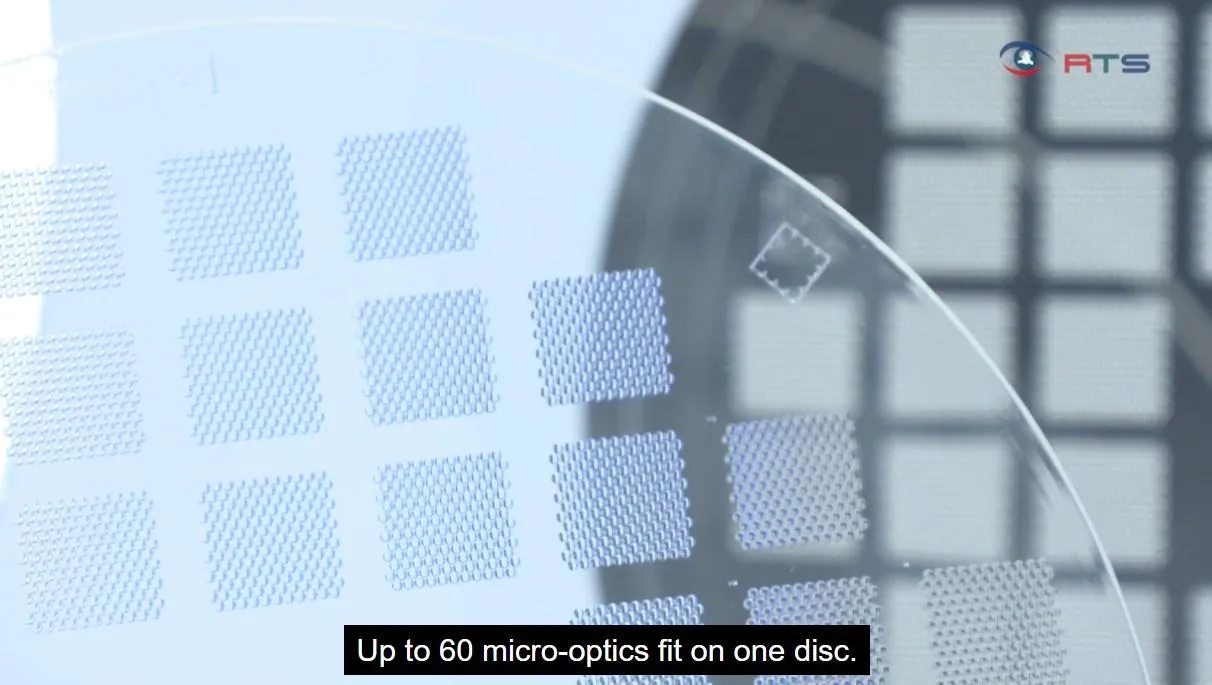
Sony repurposes PlayStation disc factory for optical microlenses

💡Sony's pivot to microlenses suggests a strategic move into next-gen hardware components for AR/VR and AI sensing.
⚡ 30-Second TL;DR
What Changed
Sony's Thalgau plant will reduce disc production to 10% of current volume by 2028.
Why It Matters
This shift signals the final decline of physical gaming media and highlights Sony's strategic pivot toward high-precision optical components, which are essential for hardware like AR/VR headsets and advanced sensors.
What To Do Next
Monitor Sony's patent filings and hardware supply chain announcements to identify potential new optical sensor technologies for future AR/VR integration.
🧠 Deep Insight
AI-generated analysis for this event.
🔑 Enhanced Key Takeaways
- •The Thalgau facility, operated by Sony DADC (Digital Audio Disc Corporation), has been a cornerstone of European physical media distribution for PlayStation consoles since the mid-1990s.
- •Sony is leveraging its proprietary mastering and replication technology, originally designed for high-density Blu-ray discs, to achieve the precision required for microlens array (MLA) fabrication.
- •The transition is part of a broader Sony Group strategy to diversify its semiconductor and sensing solutions portfolio, moving away from consumer electronics hardware reliance.
- •Microlenses produced at the plant are intended for use in advanced image sensors and AR/VR display components, aligning with Sony's dominance in the CMOS sensor market.
- •The Austrian government and local economic development agencies are providing subsidies for the workforce retraining program to prevent regional unemployment.
📊 Competitor Analysis▸ Show
| Competitor | Technology Focus | Market Position |
|---|---|---|
| Zeiss | High-precision optical components | Industry leader in lithography optics |
| Canon | Nanoimprint lithography & optics | Major supplier of semiconductor optics |
| HOYA Corporation | Optical glass & microlens arrays | Key competitor in sensor-grade optics |
🛠️ Technical Deep Dive
- The manufacturing process utilizes nanoimprint lithography (NIL) techniques adapted from optical disc mastering.
- Microlens arrays are being fabricated on high-refractive-index glass and polymer substrates to improve light-gathering efficiency in CMOS sensors.
- The facility is implementing cleanroom upgrades to meet ISO Class 5 standards, necessary for sub-micron optical fabrication.
- The process involves high-precision UV-curing resin deposition to form lens geometries with nanometer-scale surface roughness tolerances.
🔮 Future ImplicationsAI analysis grounded in cited sources
⏳ Timeline
Weekly AI Recap
Read this week's curated digest of top AI events →
👉Related Updates


AI-curated news aggregator. All content rights belong to original publishers.
Original source: The Verge ↗