🇨🇳cnBeta (Full RSS)•Freshcollected in 11m
Sony Austria Factory Pivots to Micro-lenses
💡Sony's shift to micro-lenses signals potential hardware supply chain changes for future spatial computing and AI sensors
⚡ 30-Second TL;DR
What Changed
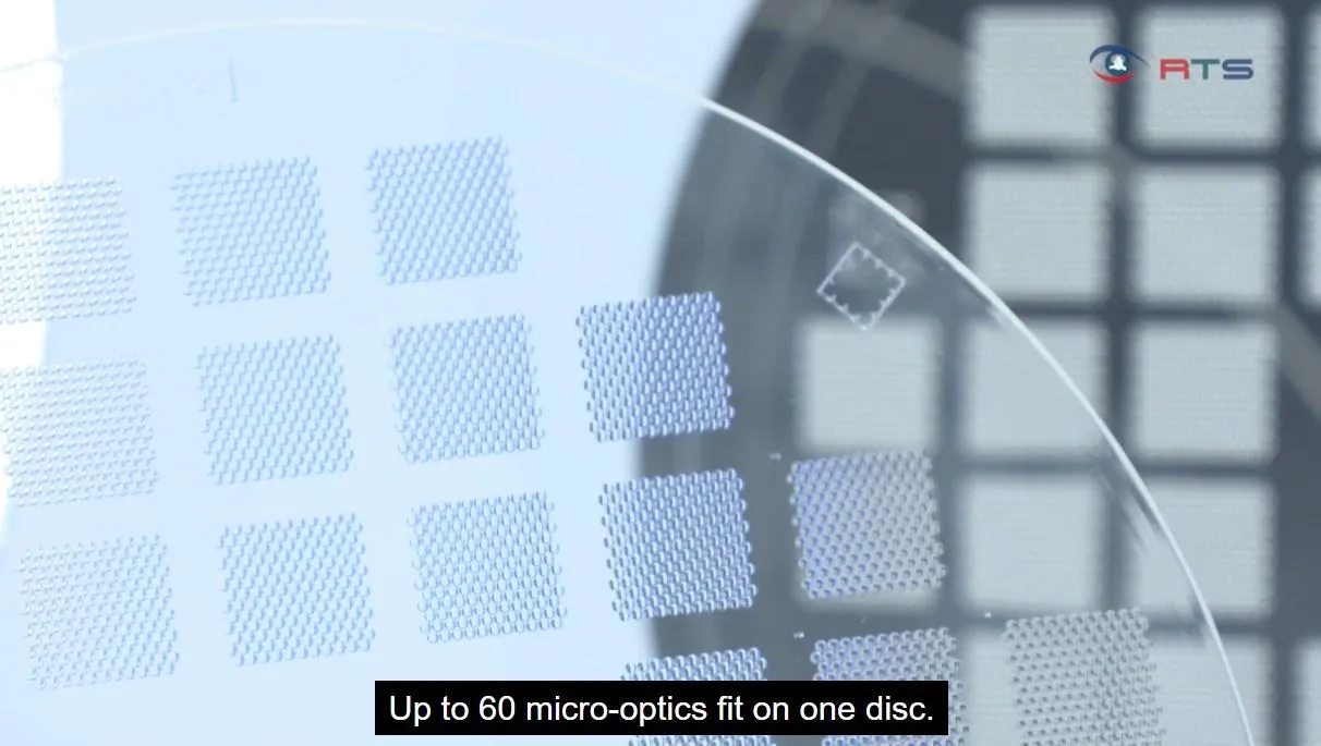
Sony DADC Thalgau factory shifting from discs to micro-lenses
Why It Matters
The pivot to micro-lenses suggests Sony is strengthening its supply chain for advanced optical components, which are critical for future AR/VR and sensor-based AI hardware.
What To Do Next
Investigate micro-lens technology specs if you are developing hardware for spatial computing or computer vision applications.
Who should care:Developers & AI Engineers
🧠 Deep Insight
AI-generated analysis for this event.
🔑 Enhanced Key Takeaways
- •The Thalgau facility, operated by Sony DADC (Digital Audio Disc Corporation), has historically served as a primary manufacturing hub for PlayStation physical media, including Blu-ray discs for PS4 and PS5.
- •The transition to micro-lenses is part of Sony's broader 'Green Management 2025' initiative, aiming to reduce environmental impact by repurposing existing industrial infrastructure rather than decommissioning sites.
- •Micro-lenses produced at the facility are intended for integration into Sony's next-generation AR/VR headsets and high-end automotive sensor arrays, moving the company into the high-growth photonics market.
- •The retraining program for the 300 employees is being conducted in partnership with local Austrian technical universities to certify staff in cleanroom operations and nanophotonic manufacturing processes.
- •Sony DADC's pivot signifies the end of an era for the Thalgau plant, which was established in 1987 and became one of the largest optical disc manufacturing sites in Europe.
🛠️ Technical Deep Dive
- The new production line utilizes nano-imprint lithography (NIL) technology to mass-produce micro-lens arrays with sub-micron precision.
- The manufacturing process involves high-precision injection molding of specialized optical polymers capable of maintaining refractive index stability under extreme thermal conditions.
- The facility is being upgraded to ISO Class 5 cleanroom standards to accommodate the sensitivity requirements of semiconductor-grade optical component fabrication.
🔮 Future ImplicationsAI analysis grounded in cited sources
Sony will cease all internal optical disc manufacturing by 2029.
The 90% volume reduction by 2028 suggests that maintaining the remaining 10% of capacity will become economically unviable for in-house production.
Sony's AR/VR hardware margins will improve due to vertical integration of optical components.
By manufacturing micro-lenses in-house at the Thalgau facility, Sony reduces reliance on third-party optical suppliers and captures more value in the headset supply chain.
⏳ Timeline
1987-01
Sony DADC establishes the Thalgau, Austria facility to manufacture CDs for the European market.
2000-03
The Thalgau plant begins mass production of PlayStation 2 optical discs.
2013-11
The facility scales up production to support the global launch of the PlayStation 4 Blu-ray media.
2020-11
Thalgau serves as a key distribution and manufacturing node for the PlayStation 5 physical disc launch.
2025-06
Sony announces the strategic restructuring of its DADC division to focus on high-precision optical components.
📰
Weekly AI Recap
Read this week's curated digest of top AI events →
👉Related Updates


AI-curated news aggregator. All content rights belong to original publishers.
Original source: cnBeta (Full RSS) ↗