🏠IT之家•Freshcollected in 3m
Infineon Opens World's Largest Power Semiconductor Fab

💡Critical infrastructure news: New capacity for power semiconductors essential for scaling AI data centers.
⚡ 30-Second TL;DR
What Changed
5 billion euro investment, the largest in Infineon's history.
Why It Matters
The increased supply of power semiconductors is vital for scaling AI data center infrastructure, which is currently facing power delivery bottlenecks.
What To Do Next
Monitor Infineon's product roadmap for new power management ICs optimized for high-density AI server racks.
Who should care:Enterprise & Security Teams
🧠 Deep Insight
AI-generated analysis for this event.
🔑 Enhanced Key Takeaways
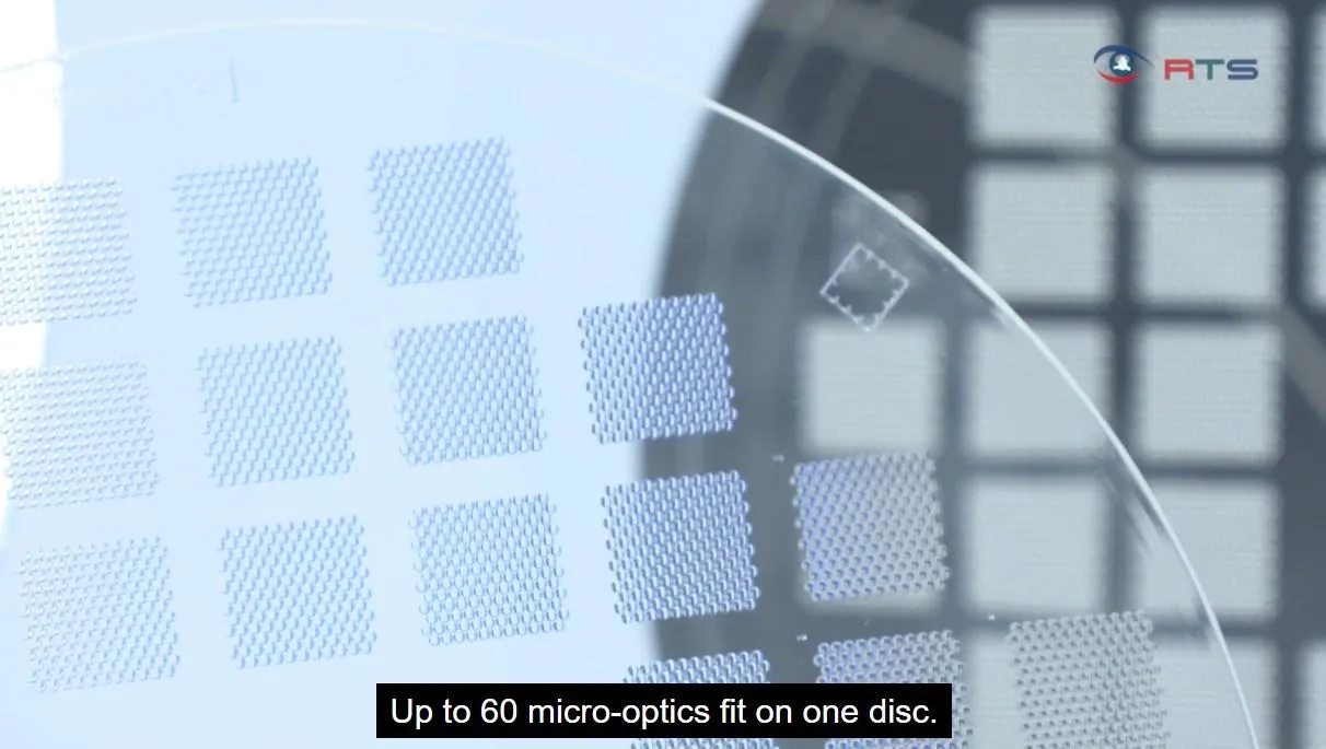
- •The facility, known as the 'Smart Power Fab,' focuses specifically on 300-millimeter (12-inch) wafer technology to maximize cost-efficiency in power semiconductor manufacturing.
- •The project received significant backing through the European Chips Act, marking it as a flagship initiative for European semiconductor sovereignty.
- •Infineon integrated advanced automation and AI-driven predictive maintenance to achieve a high degree of 'lights-out' manufacturing capability.
- •The fab is designed to be highly energy-efficient, utilizing heat recovery systems and renewable energy sources to align with Infineon's carbon neutrality goals by 2030.
- •This expansion is part of a broader strategy to address the global supply-demand imbalance for power electronics, specifically targeting the transition to electric vehicles (EVs) and industrial automation.
📊 Competitor Analysis▸ Show
| Competitor | Focus Area | Key Advantage | Technology Node |
|---|---|---|---|
| STMicroelectronics | Automotive/Industrial | Vertical integration in SiC | 200mm/300mm |
| Wolfspeed | Silicon Carbide (SiC) | Pure-play SiC leadership | 200mm |
| Texas Instruments | Analog/Power | Massive global fab footprint | 300mm |
| ON Semiconductor | Power/Sensing | Efficient SiC/IGBT portfolio | 300mm |
🛠️ Technical Deep Dive
- Wafer Size: 300mm (12-inch) production line for power semiconductors.
- Manufacturing Process: Highly automated CMOS and power-discrete hybrid processes.
- Digital Twin Integration: Real-time synchronization between physical fab operations and virtual models to optimize throughput and yield.
- AI Implementation: Machine learning algorithms used for real-time defect detection and predictive maintenance of lithography and etching equipment.
- Energy Management: Closed-loop water cooling and heat recovery systems integrated into the building infrastructure.
🔮 Future ImplicationsAI analysis grounded in cited sources
Infineon will capture a larger share of the global SiC (Silicon Carbide) market by 2028.
The increased 300mm capacity significantly lowers the per-unit cost of SiC devices, making them more competitive against traditional silicon-based power components.
The Dresden site will become the primary hub for European automotive power supply chains.
By centralizing high-volume production within the EU, Infineon reduces reliance on Asian manufacturing hubs, appealing to European automakers seeking supply chain resilience.
⏳ Timeline
2021-09
Infineon completes the expansion of its existing 300mm thin-wafer power semiconductor fab in Villach, Austria.
2022-11
Infineon announces the official groundbreaking for the new 300mm Smart Power Fab in Dresden.
2023-02
European Commission approves the project under the IPCEI (Important Project of Common European Interest) on Microelectronics.
2025-05
Infineon begins pilot production and equipment calibration at the new Dresden facility.
2026-06
Infineon officially inaugurates the full-scale Smart Power Fab in Dresden.
📰
Weekly AI Recap
Read this week's curated digest of top AI events →
👉Related Updates

AI-curated news aggregator. All content rights belong to original publishers.
Original source: IT之家 ↗