SK hynix Targets HBM5’s Thickness Wall
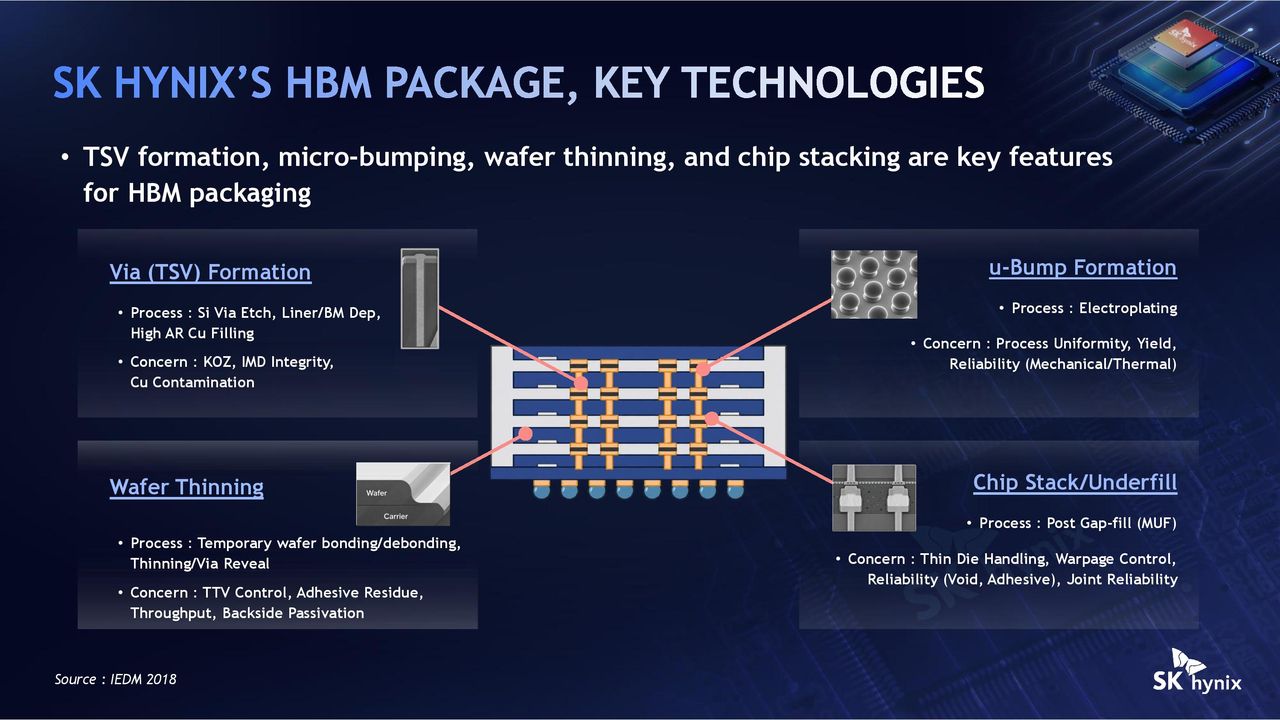
💡HBM5 packaging limits could shape the memory bandwidth and capacity available to future AI accelerators.
⚡ 30-Second TL;DR
What Changed
HBM cubes are reportedly capped at a total thickness of 775 microns.
Why It Matters
Higher-density HBM is essential for scaling AI accelerators, but package thickness and manufacturing constraints could limit future capacity gains. Hybrid bonding may help SK hynix increase stack density while addressing the physical limits of conventional packaging.
What To Do Next
When planning next-generation inference hardware, benchmark memory bandwidth and capacity assumptions against HBM5 hybrid-bonding roadmaps and Nvidia Rubin availability.
Key Points
- •HBM cubes are reportedly capped at a total thickness of 775 microns.
- •SK hynix is evaluating hybrid bonding as a future HBM5 stacking technology.
- •MR-MUF packaging is expected to remain in use through Nvidia Rubin products.
🧠 Deep Insight
Background and context from public sources — not the original article. 11 sources cited.
🔑 Enhanced Key Takeaways
- •SK hynix has introduced 'iHBM' technology, which incorporates silicon-based cooling elements directly into the memory package to achieve a 30% reduction in thermal resistance.
- •The 775-micron thickness constraint is dictated by the standard thickness of a 300mm logic wafer, necessitating thinner dies and tighter vertical spacing as layer counts grow.
- •SK hynix has confirmed that hybrid bonding will not be implemented in HBM4E, deferring its integration to the HBM5 generation.
- •The company is diversifying its AI-focused memory portfolio beyond HBM by developing High Bandwidth Flash (HBF) to optimize AI inference workloads.
- •Industry-wide HBM production capacity for the entirety of 2027 is already fully booked and sold out, reflecting extreme market demand.
📊 Competitor Analysis▸ Show
| Feature | SK hynix | Samsung |
|---|---|---|
| Primary Packaging | MR-MUF / iHBM | Custom HBM (cHBM) / zHBM |
| Strategy | Thermal management via integrated cooling | Power efficiency via advanced logic base dies |
🛠️ Technical Deep Dive
- iHBM: Integrates silicon-based cooling elements within the memory stack to lower thermal resistance by 30%.
- HBM5 Projections: Potential for 60GB capacity and 6 TB/s bandwidth, likely requiring 20-high die stacking.
- Hybrid Bonding: Eliminates traditional solder bumps by enabling direct copper-to-copper interconnection.
- MR-MUF: Mass Reflow Molded Underfill process used for die stacking to ensure mechanical and thermal stability.
🔮 Future ImplicationsAI analysis grounded in cited sources
⏳ Timeline
📎 Sources (11)
Factual claims are grounded in the sources below. Forward-looking analysis is AI-generated interpretation.
Weekly AI Recap
Read this week's curated digest of top AI events →
👉Related Updates

AI-curated news aggregator. All content rights belong to original publishers.
Original source: Tom's Hardware ↗
This is a summary, not the original. Read the source, or get the weekly briefing.
Weekly AI briefing
One email a week. Unsubscribe anytime.