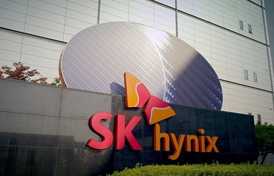
SK Hynix joins $1T club amid AI chip boom
💡Understand the massive market shift in AI infrastructure as memory manufacturers hit trillion-dollar valuations.
⚡ 30-Second TL;DR
What Changed
SK Hynix market cap exceeded 1.06 trillion USD.
Why It Matters
This confirms the critical role of memory hardware in the AI infrastructure stack, signaling sustained demand for HBM and related technologies.
What To Do Next
Monitor HBM supply chain availability as it remains a primary bottleneck for scaling large-scale AI model training.
Key Points
- •SK Hynix market cap exceeded 1.06 trillion USD.
- •Growth is driven by the global AI-focused chip demand.
- •Stock price has more than tripled year-to-date.
- •Now ranks alongside Nvidia and TSMC in valuation.
🧠 Deep Insight
Web-grounded analysis with 15 cited sources.
🔑 Enhanced Key Takeaways
- •SK Hynix is the second South Korean company to cross the $1 trillion market valuation, following Samsung Electronics earlier this month, and closely after Micron Technology also reached this milestone, indicating a broader AI-driven rally in the memory chip sector.
- •SK Hynix has maintained a dominant position in the High Bandwidth Memory (HBM) market, holding approximately 62% market share in Q2 2025 and serving as Nvidia's primary HBM supplier for its high-end GPUs.
- •The company recently introduced iHBM (Integrated High Bandwidth Memory), a new cooling solution that embeds Integrated Cooling Elements (ICEs) directly within the HBM package to reduce thermal resistance by over 30%.
- •Analysts predict that memory chip demand, especially for HBM products, will continue to outpace supply through 2028, contributing to sustained high prices and profitability for manufacturers.
- •SK Hynix's success is partly attributed to its superior MR-MUF (Mass Reflow Molded Underfill) packaging technology, which offers better heat dissipation and stacking density for HBM compared to competitors' TC-NCF methods.
📊 Competitor Analysis▸ Show
| Feature/Metric | SK Hynix | Samsung Electronics | Micron Technology |
|---|---|---|---|
| HBM Market Share (Q2 2025) | ~62% | ~17% | ~21% |
| Key HBM Generations | HBM3, HBM3E (mass production leader), HBM4 (development/sampling) | HBM3E, HBM4 (expected Q1 2026 for Nvidia Rubin) | HBM3E, HBM4 (sampling) |
| Packaging Technology | MR-MUF (Mass Reflow Molded Underfill) | TC-NCF (Thermal Compression with Non-Conductive Film) | TC-NCF (Thermal Compression with Non-Conductive Film) |
| AI Chip Supply | Primary HBM supplier for Nvidia | Supply contracts with AI major Nvidia | Supply contracts with AI major Nvidia |
| Recent Innovation | iHBM (Integrated Cooling Elements) | Investing in advanced nodes and packaging | Strong patent portfolio, hybrid bonding, through-silicon trench cooling |
🛠️ Technical Deep Dive
- High Bandwidth Memory (HBM) is a computer memory interface for 3D-stacked synchronous dynamic random-access memory (SDRAM).
- HBM utilizes Through-Silicon Vias (TSVs) to directly connect multiple DRAM dies, significantly increasing memory bandwidth and reducing data travel distance.
- SK Hynix developed the world's first HBM memory chip in 2013 and has been a pioneer in subsequent generations.
- HBM3 offers I/O speeds of 5.2 Gbit/s and a bandwidth of 665 GB/s per package, supporting up to 16-high 2.5D and 3D solutions.
- SK Hynix's HBM3E achieves 8 Gbit/s/pin data processing speed, which is 25% faster than HBM3, and delivers a bandwidth of 1 TB/s per stack.
- The newly introduced iHBM (Integrated High Bandwidth Memory) solution embeds Integrated Cooling Elements (ICEs) directly within the HBM package, reducing thermal resistance by over 30% compared to traditional indirect cooling methods. This technology targets thermal hotspots in the Die-to-Die Physical Layer (D2D PHY) area.
- SK Hynix employs MR-MUF (Mass Reflow Molded Underfill) packaging technology, which is noted for superior heat dissipation and stacking density in HBM products.
- The upcoming HBM4 standard is expected to double the number of channels per stack from 8 to 16 and achieve significantly faster I/O per pin, targeting 12–16 Gbps per pin and 1.5–2.0 TB/s bandwidth per stack.
🔮 Future ImplicationsAI analysis grounded in cited sources
⏳ Timeline
📎 Sources (15)
Factual claims are grounded in the sources below. Forward-looking analysis is AI-generated interpretation.
Weekly AI Recap
Read this week's curated digest of top AI events →
👉Related Updates
Same topic
Explore #hbm
Same product
More on sk-hynix-memory-chips
Same source
Latest from cnBeta (Full RSS)

PACA: Open-source tool for ancient fossil coordinate mapping

First atmosphere detected on habitable-zone exoplanet

Samsung Secures $200B Broadcom AI Infrastructure Deal
How AMD's 2006 ATI Acquisition Built Today's AI Empire
AI-curated news aggregator. All content rights belong to original publishers.
Original source: cnBeta (Full RSS) ↗