SK Hynix to Double Memory Capacity by 2030
💡Critical supply chain insight: AI memory shortages will impact infrastructure costs through 2030.
⚡ 30-Second TL;DR
What Changed
SK Hynix to double memory wafer capacity in 5 years
Why It Matters
The extended supply shortage suggests that AI infrastructure costs will remain high for developers and enterprises. Long-term hardware planning is essential to mitigate potential bottlenecks in model training.
What To Do Next
Adjust your hardware procurement roadmap to account for long-term memory supply constraints and premium pricing.
Key Points
- •SK Hynix to double memory wafer capacity in 5 years
- •AI-driven demand is the primary driver for expansion
- •Global memory shortage expected to last until 2030
🧠 Deep Insight
Background and context from public sources — not the original article. 18 sources cited.
🔑 Enhanced Key Takeaways
- •SK Hynix currently holds a dominant position in the global High Bandwidth Memory (HBM) market, with a 58% share in the first quarter of 2026, significantly outpacing rivals Samsung Electronics and Micron Technology, each holding 21%.
- •The company's planned expansion will involve investments well above the 30.2 trillion won (approximately $20 billion) spent in 2025, though an exact figure for the new capacity buildout was not disclosed.
- •SK Hynix has already sold out its entire memory production capacity for 2026, with some customers reportedly offering to pre-fund fab lines and purchase advanced EUV scanners to secure future supply.
- •The capacity expansion includes plans for its M15X fab in Cheongju, South Korea, the Yongin semiconductor cluster, and new advanced packaging facilities in the United States.
- •SK Hynix's market capitalization recently surpassed $1 trillion for the first time, joining Samsung Electronics and Micron Technology in reaching this milestone, driven by the AI-fueled rally.
📊 Competitor Analysis▸ Show
Competitor Analysis: High Bandwidth Memory (HBM) Market
| Feature/Metric | SK Hynix | Samsung Electronics | Micron Technology |
|---|---|---|---|
| HBM Market Share (Q1 2026) | 58% | 21% | 21% |
| HBM Market Share (Q2/Q3 2025) | 57-62% | 17-22% | 21% |
| HBM3E Production | First to mass-produce HBM3E, shipped 36GB in Q3 2023, 48GB in Q4 2024 | Ramping aggressively, improving yield, shipping HBM4E samples | Entered later, secured allocation with AI chip vendors |
| HBM4 Roadmap | Targeting 12-16 Gbps/pin, 1.5-2.0 TB/s, 64-128 GB capacity, mass production 2026 | Positioning 6th-gen 10nm-class DRAM for HBM4 volume | Targeting 12-16 Gbps/pin, 1.5-2.0 TB/s, 64-128 GB capacity, mass production 2026-2027 |
| Key Customer Relationships | Primary supplier for NVIDIA (H100, H200, B100/B200) | Qualifying HBM3E parts with major customers | Secured allocation with several AI chip vendors |
| Overall DRAM Market Share (Q1 2025) | 36% (ranked 1st) | 34% (ranked 2nd) | 25% (ranked 3rd) |
| Advanced Packaging | Utilizes MR-MUF and TSV technology | Introduced Heat Path Block (HPB) thermal management | Leveraging early EUV adoption |
🛠️ Technical Deep Dive
- HBM3E Technology: SK Hynix's HBM3E modules deliver 9.2 Gbps per pin, achieving 1 TB/s bandwidth per stack and up to 24GB capacity per stack. The company shipped 36GB HBM3E in Q3 2023 and 48GB variants in Q4 2024, reaching 9.6 Gbps per pin and 1.15 TB/s bandwidth per stack.
- HBM4 Development: Expected in 2025-2026, HBM4 is projected to offer 1.5+ TB/s per stack with up to 48GB capacity, utilizing a new base-logic die architecture. SK Hynix and Micron are targeting 12-16 Gbps per pin (PAM-4 signaling), 1.5-2.0 TB/s bandwidth per stack, and 64-128 GB capacity via 16-hi die stacking.
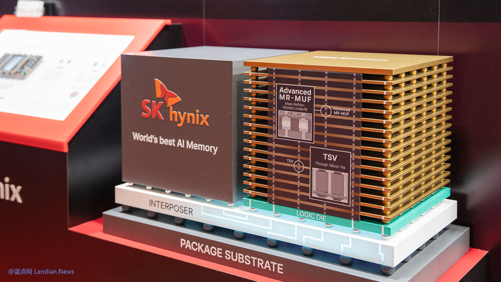
- Advanced Packaging: SK Hynix employs Through-Silicon Via (TSV) stacking lines and Mass Reflow Molded Underfill (MR-MUF) technology. MR-MUF uses a liquid epoxy molding compound with enhanced thermal conductivity, which helps manage heat and prevent die warping, enabling the reliable production of 12-high HBM3E modules.
- Manufacturing Process: The investment also supports the migration to 1β and 1γ DRAM process nodes and the expansion of Extreme Ultraviolet (EUV) lithography layers, crucial for manufacturing next-generation chips.
🔮 Future ImplicationsAI analysis grounded in cited sources
⏳ Timeline
📎 Sources (18)
Factual claims are grounded in the sources below. Forward-looking analysis is AI-generated interpretation.
Weekly AI Recap
Read this week's curated digest of top AI events →
👉Related Updates
AI-curated news aggregator. All content rights belong to original publishers.
Original source: cnBeta (Full RSS) ↗
This is a summary, not the original. Read the source, or get the weekly briefing.
The weekly digest
One email a week. Unsubscribe anytime.