來源cnBeta (Full RSS)•較早收集於 4m
SK Hynix 計畫在 2030 年前將記憶體產能翻倍
💡關鍵供應鏈洞察:AI 記憶體短缺將影響基礎設施成本至 2030 年。
⚡ 30 秒速覽
有什麼變化
SK Hynix 將在五年內將記憶體晶圓產能翻倍
為什麼重要
持續的供應短缺意味著開發者與企業的 AI 基礎設施成本將維持高檔。長期硬體規劃對於緩解模型訓練中的潛在瓶頸至關重要。
下一步行動
調整您的硬體採購路線圖,以應對長期的記憶體供應限制與高昂價格。
誰應關注:Enterprise & Security Teams
關鍵要點
- •SK Hynix 將在五年內將記憶體晶圓產能翻倍
- •AI 驅動的需求是產能擴張的主要動力
- •全球記憶體短缺預計將持續至 2030 年
🧠 深度解析
背景與延伸:來自公開資料,非原文內容。引用 18 個來源。
🔑 增強重點摘要
- •SK Hynix currently holds a dominant position in the global High Bandwidth Memory (HBM) market, with a 58% share in the first quarter of 2026, significantly outpacing rivals Samsung Electronics and Micron Technology, each holding 21%.
- •The company's planned expansion will involve investments well above the 30.2 trillion won (approximately $20 billion) spent in 2025, though an exact figure for the new capacity buildout was not disclosed.
- •SK Hynix has already sold out its entire memory production capacity for 2026, with some customers reportedly offering to pre-fund fab lines and purchase advanced EUV scanners to secure future supply.
- •The capacity expansion includes plans for its M15X fab in Cheongju, South Korea, the Yongin semiconductor cluster, and new advanced packaging facilities in the United States.
- •SK Hynix's market capitalization recently surpassed $1 trillion for the first time, joining Samsung Electronics and Micron Technology in reaching this milestone, driven by the AI-fueled rally.
📊 競品分析▸ Show
Competitor Analysis: High Bandwidth Memory (HBM) Market
| Feature/Metric | SK Hynix | Samsung Electronics | Micron Technology |
|---|---|---|---|
| HBM Market Share (Q1 2026) | 58% | 21% | 21% |
| HBM Market Share (Q2/Q3 2025) | 57-62% | 17-22% | 21% |
| HBM3E Production | First to mass-produce HBM3E, shipped 36GB in Q3 2023, 48GB in Q4 2024 | Ramping aggressively, improving yield, shipping HBM4E samples | Entered later, secured allocation with AI chip vendors |
| HBM4 Roadmap | Targeting 12-16 Gbps/pin, 1.5-2.0 TB/s, 64-128 GB capacity, mass production 2026 | Positioning 6th-gen 10nm-class DRAM for HBM4 volume | Targeting 12-16 Gbps/pin, 1.5-2.0 TB/s, 64-128 GB capacity, mass production 2026-2027 |
| Key Customer Relationships | Primary supplier for NVIDIA (H100, H200, B100/B200) | Qualifying HBM3E parts with major customers | Secured allocation with several AI chip vendors |
| Overall DRAM Market Share (Q1 2025) | 36% (ranked 1st) | 34% (ranked 2nd) | 25% (ranked 3rd) |
| Advanced Packaging | Utilizes MR-MUF and TSV technology | Introduced Heat Path Block (HPB) thermal management | Leveraging early EUV adoption |
🛠️ 技術深入
- HBM3E Technology: SK Hynix's HBM3E modules deliver 9.2 Gbps per pin, achieving 1 TB/s bandwidth per stack and up to 24GB capacity per stack. The company shipped 36GB HBM3E in Q3 2023 and 48GB variants in Q4 2024, reaching 9.6 Gbps per pin and 1.15 TB/s bandwidth per stack.
- HBM4 Development: Expected in 2025-2026, HBM4 is projected to offer 1.5+ TB/s per stack with up to 48GB capacity, utilizing a new base-logic die architecture. SK Hynix and Micron are targeting 12-16 Gbps per pin (PAM-4 signaling), 1.5-2.0 TB/s bandwidth per stack, and 64-128 GB capacity via 16-hi die stacking.
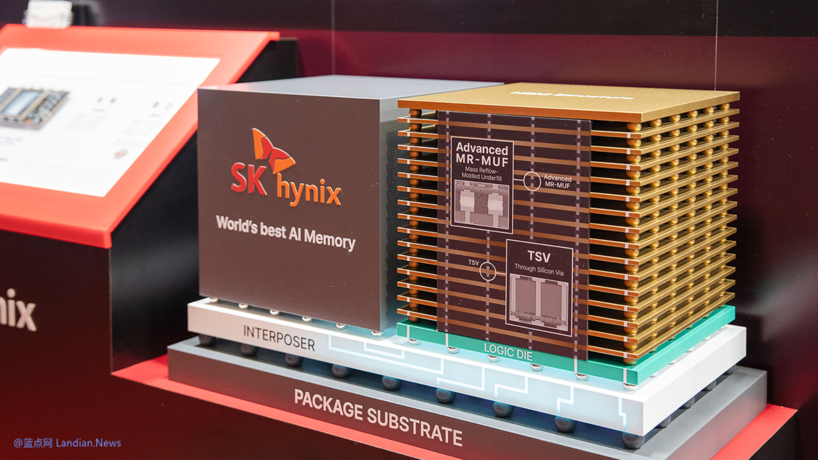
- Advanced Packaging: SK Hynix employs Through-Silicon Via (TSV) stacking lines and Mass Reflow Molded Underfill (MR-MUF) technology. MR-MUF uses a liquid epoxy molding compound with enhanced thermal conductivity, which helps manage heat and prevent die warping, enabling the reliable production of 12-high HBM3E modules.
- Manufacturing Process: The investment also supports the migration to 1β and 1γ DRAM process nodes and the expansion of Extreme Ultraviolet (EUV) lithography layers, crucial for manufacturing next-generation chips.
🔮 前景展望基於引用來源的 AI 分析
SK Hynix will likely solidify its leadership in the HBM market.
Its aggressive capacity expansion, early mass production of HBM3E, and strong co-development relationship with NVIDIA position it favorably against competitors in the rapidly growing AI memory sector.
The memory industry's valuation logic is shifting from a cyclical commodity to a strategic AI core asset.
AI-driven demand is creating sustained shortages, higher margins for HBM, and long-term supply contracts, fundamentally transforming the market dynamics compared to traditional memory cycles.
AI infrastructure development will face continued memory bottlenecks despite significant investments.
The lead time for constructing new fabrication plants (fabs) is over five years, meaning that new supply will only come online towards the end of the predicted shortage window, and supply growth is unlikely to match the rapid pace of AI infrastructure buildouts in the near term.
⏳ 時間線
1983
Construction of first semiconductor fabrication factory (as Hyundai Electronics).
2013
Co-developed the world's first High Bandwidth Memory (HBM).
2018-2019
Shipped first HBM2E (Aquabolt) memory.
2022-Q4
Began first HBM3 production shipments.
2023-Q3
Entered volume production of 36 GB HBM3E memory.
2025-Q1
Overtook Samsung in overall DRAM market share.
2026-02
Announced $15 billion investment to expand next-generation memory manufacturing, focusing on HBM.
2026-05
Market capitalization surpassed $1 trillion for the first time.
📎 來源 (18)
Factual claims are grounded in the sources below. Forward-looking analysis is AI-generated interpretation.
📰
AI 週報
閱讀本週精選 AI 大事摘要 →
👉相關動態
AI 策展新聞聚合。所有內容版權歸原始發布者所有。
原始來源: cnBeta (Full RSS) ↗
每週電子報
每週一封,可隨時退訂。