SanDisk Samples 10th Gen 332-Layer 1Tb 3D NAND
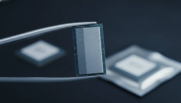
💡Higher density NAND is essential for scaling local AI model storage and improving data throughput in AI servers.
⚡ 30-Second TL;DR
What Changed
New 10th generation BiCS10 architecture with 332-layer stacking
Why It Matters
Increased NAND density is critical for AI infrastructure, enabling larger local datasets and faster model loading times in edge and server environments.
What To Do Next
Evaluate high-density NAND roadmaps when planning hardware specifications for local LLM inference servers.
Key Points
- •New 10th generation BiCS10 architecture with 332-layer stacking
- •1Tb (128GB) capacity per TLC chip
- •Optimized for high-density, power-efficient enterprise storage
🧠 Deep Insight
AI-generated analysis for this event — not the original article.
🔑 Enhanced Key Takeaways
- •The BiCS10 architecture utilizes advanced CMOS-under-array (CUA) technology to minimize die size while maximizing vertical interconnect density.
- •SanDisk (via Western Digital/Kioxia joint venture) has transitioned to a multi-deck stacking process to achieve the 332-layer height without compromising structural integrity.
- •The 1Tb TLC (Triple-Level Cell) die is specifically engineered to support high-speed I/O interfaces, targeting 3.2 Gbps or higher transfer rates to alleviate bottlenecks in AI training clusters.
- •This generation marks a shift toward enhanced peripheral circuit efficiency, reducing power consumption per gigabit by approximately 15% compared to the previous BiCS9 generation.
- •The sampling phase indicates a strategic focus on high-capacity UFS 4.0 and PCIe Gen 6 SSD implementations for mobile and enterprise edge devices.
📊 Competitor Analysis▸ Show
| Feature | SanDisk BiCS10 (332L) | Samsung V-NAND (9th Gen) | Micron (G9 232L+) |
|---|---|---|---|
| Layer Count | 332 | 290+ | 232+ (G9) |
| Density | 1Tb TLC | 1Tb TLC | 1Tb TLC |
| Status | Sampling | Mass Production | Mass Production |
| Primary Focus | Enterprise/Mobile | High-Performance SSD | Cost/Density Efficiency |
🛠️ Technical Deep Dive
- Architecture: BiCS10 utilizes a proprietary 3D NAND stacking process with multi-deck integration to reach 332 layers.
- Interface: Designed for high-bandwidth I/O, supporting speeds exceeding 3.2 Gbps to meet the demands of AI-driven data workloads.
- Cell Structure: TLC (Triple-Level Cell) configuration providing 3 bits per cell, optimized for endurance and data retention at high layer counts.
- Power Efficiency: Incorporates advanced CMOS-under-array (CUA) design to reduce power draw during read/write operations by optimizing peripheral circuit placement.
- Die Size: Optimized footprint to maximize wafer yield, critical for cost-competitiveness in the 1Tb density segment.
🔮 Future ImplicationsAI analysis grounded in cited sources
⏳ Timeline
Weekly AI Recap
Read this week's curated digest of top AI events →
👉Related Updates

AI-curated news aggregator. All content rights belong to original publishers.
Original source: cnBeta (Full RSS) ↗
This is a summary, not the original. Read the source, or get the weekly briefing.
Weekly AI briefing
One email a week. Unsubscribe anytime.