Samsung Teases HBM5 at 4 TB/s per Stack
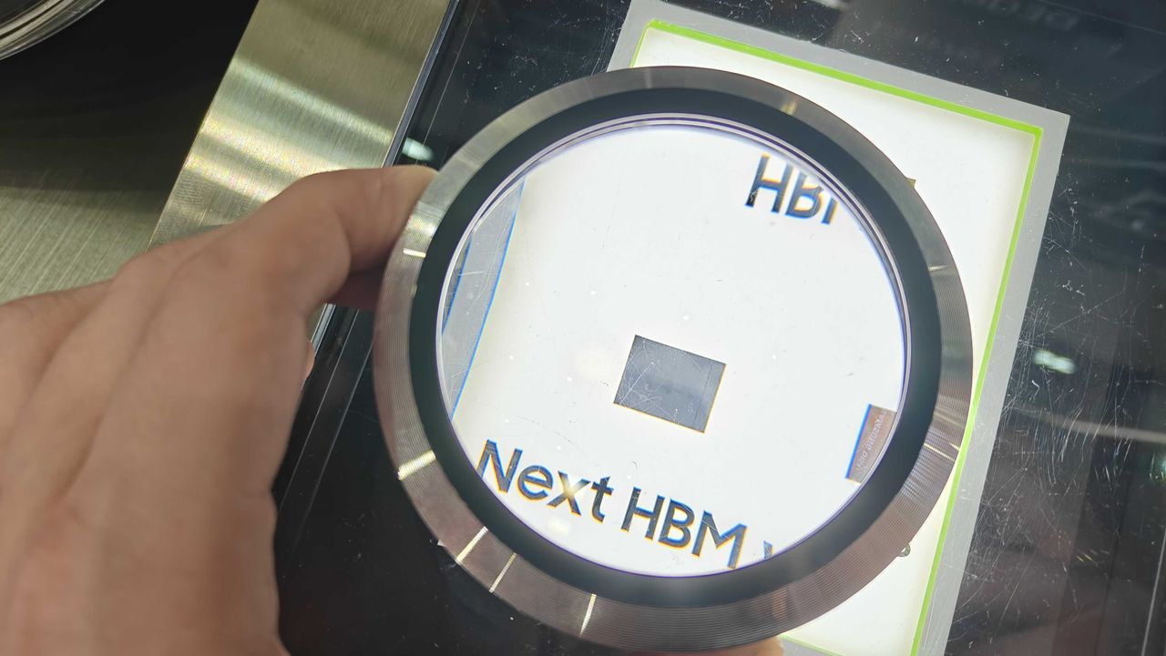
💡Samsung's HBM5 roadmap points to a major leap in AI accelerator memory bandwidth.
⚡ 30-Second TL;DR
What Changed
Samsung projects 4 TB/s of bandwidth per HBM5 stack by the late 2020s.
Why It Matters
HBM5 could reduce memory-bandwidth bottlenecks in large AI training and inference systems. It may also encourage accelerator designers to target much wider interfaces and more aggressively scale model throughput.
What To Do Next
Model your next AI accelerator's memory-bound workloads at 4 TB/s per HBM5 stack and compare the projected gains against HBM4E-based designs.
Key Points
- •Samsung projects 4 TB/s of bandwidth per HBM5 stack by the late 2020s.
- •HBM5 is expected to deliver roughly twice the performance of HBM4E.
- •AI accelerators could reach aggregate memory bandwidth of around 100 TB/s.
🧠 Deep Insight
Background and context from public sources — not the original article. 8 sources cited.
🔑 Enhanced Key Takeaways
- •Samsung is transitioning the HBM5 base die to a proprietary 2 nm process node, a significant shift from the 4 nm nodes used in previous generations.
- •The HBM5 architecture will support diverse stacking configurations, specifically 12-layer, 16-layer, and 20-layer options to cater to varying workload requirements.
- •Samsung has introduced 'Heat Path Block' (HPB) technology, which is specifically engineered to reduce thermal resistance by 20% compared to previous HBM iterations.
- •The company is implementing a 'CUBE' development strategy, which prioritizes Capacity, Utilization, Bandwidth, and Efficiency to optimize 3D-stacked memory structures.
- •Samsung is concurrently developing 'zHBM,' a post-HBM5 architecture that stacks memory directly atop the processor to achieve an 8x performance increase over HBM4E.
📊 Competitor Analysis▸ Show
| Feature | Samsung HBM5 | NVIDIA NVHBM |
|---|---|---|
| Architecture | 3D-stacked (side-by-side) | Integrated memory controller in base die |
| Primary Focus | Bandwidth/Efficiency | Efficiency/Customization |
| Status | Roadmap (2028) | Announced/In-development |
🛠️ Technical Deep Dive
- Base Die Process: 2 nm proprietary node
- Thermal Management: Heat Path Block (HPB) technology
- Stacking Options: 12-layer, 16-layer, and 20-layer configurations
- Efficiency Metrics: 20% improvement in performance per watt over HBM4E
- Thermal Resistance: 20% reduction via HPB implementation
🔮 Future ImplicationsAI analysis grounded in cited sources
⏳ Timeline
📎 Sources (8)
Factual claims are grounded in the sources below. Forward-looking analysis is AI-generated interpretation.
Weekly AI Recap
Read this week's curated digest of top AI events →
👉Related Updates

AI-curated news aggregator. All content rights belong to original publishers.
Original source: Tom's Hardware ↗
This is a summary, not the original. Read the source, or get the weekly briefing.
Weekly AI briefing
One email a week. Unsubscribe anytime.