Hybrid Bonding Advances as HBM Hits Delay
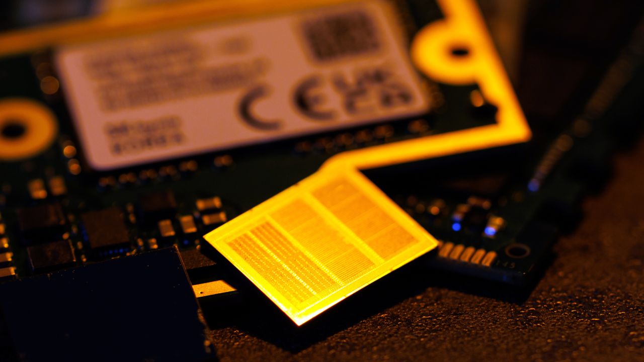
💡HBM packaging delays could reshape the timeline for denser AI accelerator memory.
⚡ 30-Second TL;DR
What Changed
Copper-to-copper hybrid bonding is replacing solder microbumps in 3D chip stacks.
Why It Matters
The delay could slow the transition to denser, higher-bandwidth memory stacks for AI accelerators. Chip designers and infrastructure buyers may need to plan for continued reliance on conventional HBM packaging timelines.
What To Do Next
Ask your accelerator and memory suppliers whether their next-generation HBM roadmaps depend on hybrid bonding before finalizing capacity plans.
Key Points
- •Copper-to-copper hybrid bonding is replacing solder microbumps in 3D chip stacks.
- •TSMC is currently operating at a 6-micron bonding pitch.
- •High-volume production has begun for logic, but HBM memory adoption has been postponed.
🧠 Deep Insight
Background and context from public sources — not the original article. 7 sources cited.
🔑 Enhanced Key Takeaways
- •JEDEC updated the HBM stack-height specifications in 2026, permitting the continued use of microbump technology for HBM4 and delaying the mandatory transition to hybrid bonding.
- •The industry is currently grappling with 'CMP dishing' and thermal management issues, specifically the requirement to maintain structural integrity under 300°C bonding temperatures.
- •SK Hynix is diversifying its advanced packaging supply chain by exploring partnerships with Intel for HBM4E base dies to reduce reliance on TSMC.
- •Samsung's 'CUBE' strategy explicitly integrates hybrid copper bonding (HCB) as a core pillar for future vertical stacking of memory and logic devices.
- •The industry has identified a 775-micron physical stack-height ceiling, which serves as the primary technical driver for eventually mandating hybrid bonding in future HBM generations.
📊 Competitor Analysis▸ Show
| Feature | TSMC (SoIC) | Samsung (CUBE) | SK Hynix (Advanced Packaging) |
|---|---|---|---|
| Bonding Pitch | 6-micron | R&D phase | R&D phase |
| Primary Focus | Logic-to-Logic/Memory | Memory-to-Logic Stacking | HBM4E/HBM5 Integration |
| Strategy | High-volume logic | Vertical integration | U.S. facility expansion |
🛠️ Technical Deep Dive
- Hybrid bonding utilizes a direct copper-to-copper interface, eliminating solder microbumps and the associated underfill materials.
- The process requires Chemical Mechanical Planarization (CMP) to achieve near-atomic flatness on die surfaces to ensure successful bonding.
- Bonding involves high-pressure and high-temperature (up to 300°C) cycles to facilitate copper diffusion across the interface.
- The transition to hybrid bonding is necessary to overcome the 775-micron stack-height limit imposed by current microbump-based packaging architectures.
🔮 Future ImplicationsAI analysis grounded in cited sources
⏳ Timeline
📎 Sources (7)
Factual claims are grounded in the sources below. Forward-looking analysis is AI-generated interpretation.
Weekly AI Recap
Read this week's curated digest of top AI events →
👉Related Updates


AI-curated news aggregator. All content rights belong to original publishers.
Original source: Tom's Hardware ↗
This is a summary, not the original. Read the source, or get the weekly briefing.
Weekly AI briefing
One email a week. Unsubscribe anytime.