Samsung Delays 1.4nm to 2029
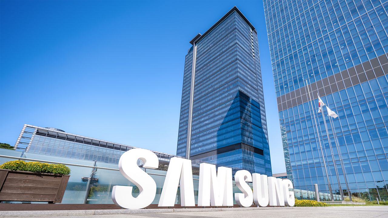
💡Samsung's delayed 1.4nm roadmap could reshape timelines and sourcing for future AI accelerators.
⚡ 30-Second TL;DR
What Changed
Samsung Foundry's 1.4nm-class node is now targeted for 2029
Why It Matters
The revised schedule signals a slower transition to sub-2nm manufacturing and may affect future AI accelerator supply planning. High-NA EUV adoption could eventually improve the economics and scalability of 1nm-class chips.
What To Do Next
Update your AI hardware roadmap to model Samsung's 2029 1.4nm availability and evaluate alternative foundries for nearer-term accelerator designs.
Key Points
- •Samsung Foundry's 1.4nm-class node is now targeted for 2029
- •SF2 is expected to remain in production for an unusually long period
- •High-NA EUV is planned for 1nm-class nodes starting in 2030
🧠 Deep Insight
AI-generated analysis for this event.
🔑 Enhanced Key Takeaways
- •Samsung's strategic pivot reflects a broader industry trend of prioritizing yield optimization and cost-efficiency in advanced nodes over aggressive, high-risk scaling timelines.
- •The delay is reportedly linked to challenges in achieving competitive power, performance, and area (PPA) metrics for the 1.4nm node compared to existing SF2 iterations.
- •Samsung is shifting focus toward 'SF2P' (2nm performance-enhanced) and 'SF2Z' (backside power delivery) variants to bridge the gap until 1nm-class production.
- •The adoption of High-NA EUV lithography is now explicitly tied to the 1nm-class node, marking a departure from earlier industry speculation that Samsung might integrate it sooner.
- •This roadmap adjustment aligns with Samsung's efforts to stabilize its foundry business unit, which has faced significant pressure from TSMC's dominance in the high-end AI chip market.
📊 Competitor Analysis▸ Show
| Feature | Samsung Foundry | TSMC | Intel Foundry |
|---|---|---|---|
| Advanced Node Strategy | Focus on SF2/SF2P/SF2Z longevity | Rapid transition to N2/N2P/A16 | Aggressive 18A and 14A adoption |
| High-NA EUV Status | Targeted for 1nm-class (2030+) | Pilot/Production integration (A16/A14) | Early adopter (High-NA tools installed) |
| Backside Power Delivery | SF2Z (Planned) | N2P (Planned) | PowerVia (Implemented) |
🛠️ Technical Deep Dive
- SF2 (2nm): Utilizes Multi-Bridge-Channel FET (MBCFET) architecture, Samsung's proprietary implementation of Gate-All-Around (GAA) transistors.
- SF2Z: Incorporates Backside Power Delivery Network (BSPDN) to reduce IR drop and improve power efficiency by separating power and signal routing.
- High-NA EUV: Refers to lithography machines with a numerical aperture of 0.55, enabling higher resolution patterning required for sub-2nm features without multi-patterning.
- 1nm-class nodes: Expected to leverage further refinements in nanosheet scaling and potentially transition to new channel materials or advanced 3D stacking techniques.
🔮 Future ImplicationsAI analysis grounded in cited sources
⏳ Timeline
Weekly AI Recap
Read this week's curated digest of top AI events →
👉Related Updates


AI-curated news aggregator. All content rights belong to original publishers.
Original source: Tom's Hardware ↗