Intel Teases a Return to Memory Innovation
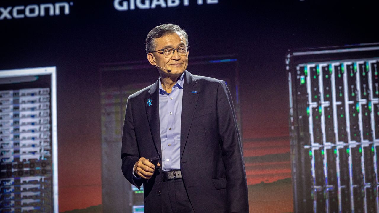
💡Intel may be exploring memory-CPU stacking that could reshape AI bandwidth and data-movement bottlenecks.
⚡ 30-Second TL;DR
What Changed
Intel may re-enter the memory business under CEO Lip-Bu Tan.
Why It Matters
A new memory architecture or tighter memory-CPU integration could improve bandwidth and reduce data movement for AI workloads. However, the comments are preliminary and do not represent a confirmed product or roadmap.
What To Do Next
Track Intel's upcoming architecture disclosures and compare any memory-stacking claims against HBM bandwidth, latency, and power metrics used in your AI accelerator designs.
Key Points
- •Intel may re-enter the memory business under CEO Lip-Bu Tan.
- •Tan described a personal project focused on a new memory architecture.
- •The concept could involve vertically stacking memory and CPUs.
- •The comments suggest potential future innovation in computing memory systems.
🧠 Deep Insight
AI-generated analysis for this event.
🔑 Enhanced Key Takeaways
- •Intel previously exited the standalone memory market in 2020 when it sold its NAND memory business, including the Solidigm brand, to SK Hynix.
- •Lip-Bu Tan's leadership marks a strategic pivot from the previous 'IDM 2.0' focus on foundry services toward re-integrating high-performance memory architectures directly into silicon design.
- •The proposed stacking architecture likely leverages advanced 3D packaging technologies, such as Foveros, to reduce latency and power consumption by minimizing the physical distance between compute and memory.
- •Industry analysts suggest this move is a response to the 'memory wall' bottleneck, where traditional DDR5/HBM interfaces limit the performance of high-core-count AI processors.
- •Intel's historical expertise in Optane (3D XPoint) technology is being re-evaluated as a foundation for this new architecture, potentially reviving non-volatile memory research for AI workloads.
📊 Competitor Analysis▸ Show
| Feature | Intel (Proposed) | NVIDIA (Grace Hopper) | AMD (MI300 Series) |
|---|---|---|---|
| Memory Integration | Direct 3D Stacking | HBM3e via Chiplets | HBM3e via Chiplets |
| Architecture Focus | Compute-Memory Fusion | GPU-Centric Memory | APU-Centric Memory |
| Primary Advantage | Potential Latency Reduction | Ecosystem/Software Stack | High Bandwidth Density |
🛠️ Technical Deep Dive
- Architecture utilizes 3D vertical stacking to integrate memory dies directly onto the CPU/GPU logic die.
- Implementation relies on Through-Silicon Vias (TSVs) to facilitate high-bandwidth, low-latency interconnects between layers.
- Design targets the elimination of traditional memory bus bottlenecks by moving memory closer to the execution units.
- Potential use of high-density, low-power memory cells optimized for AI inference and large language model (LLM) caching.
🔮 Future ImplicationsAI analysis grounded in cited sources
⏳ Timeline
Weekly AI Recap
Read this week's curated digest of top AI events →
👉Related Updates

AI-curated news aggregator. All content rights belong to original publishers.
Original source: Tom's Hardware ↗