SourcecnBeta (Full RSS)•Stalecollected in 51m
Samsung Builds Wonyang HBM Factory This Year
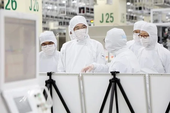
Samsung ramps HBM capacity to meet exploding AI GPU memory demand
30-Second TL;DR
What Changed
Wonyang factory construction finishes this year.
Why It Matters
Expands Samsung's HBM supply critical for AI GPUs, potentially easing shortages in AI training infrastructure and stabilizing costs for data centers.
What To Do Next
Track Samsung HBM yield improvements for AI cluster memory sourcing.
Who should care:Enterprise & Security Teams
Key Points
- •Wonyang factory construction finishes this year.
- •Advanced HBM packaging production begins next year.
- •Diversifies HBM capacity from overburdened Tianan plant.
- •Relocates Wonyang DRAM packaging to Vietnam.
Deep Insight
AI-generated analysis for this event — not the original article.
Enhanced Key Takeaways
- •The Wonyang facility transition is part of Samsung's broader 'HBM4' roadmap, aiming to integrate logic dies directly into the HBM stack using advanced 12-layer and 16-layer stacking technologies.
- •Samsung is shifting its packaging strategy to prioritize 'Advanced Packaging' (AVP) techniques, specifically utilizing hybrid bonding to improve thermal management and signal integrity for high-bandwidth AI accelerators.
- •The relocation of general DRAM lines to Vietnam is intended to optimize cost structures, allowing the South Korean domestic facilities to focus exclusively on high-margin, high-complexity AI memory products.
Competitor Analysis
Primary HBM Tech
- Samsung (Wonyang/Tianan)
- HBM3E / HBM4
- SK Hynix
- HBM3E / HBM4
- Micron
- HBM3E
Packaging Focus
- Samsung (Wonyang/Tianan)
- Hybrid Bonding / AVP
- SK Hynix
- MR-MUF
- Micron
- TCB (Thermal Compression Bonding)
Capacity Strategy
- Samsung (Wonyang/Tianan)
- Dual-track (Korea/Vietnam)
- SK Hynix
- Aggressive domestic expansion
- Micron
- Global footprint (US/Japan/Taiwan)
| Feature | Samsung (Wonyang/Tianan) | SK Hynix | Micron |
|---|---|---|---|
| Primary HBM Tech | HBM3E / HBM4 | HBM3E / HBM4 | HBM3E |
| Packaging Focus | Hybrid Bonding / AVP | MR-MUF | TCB (Thermal Compression Bonding) |
| Capacity Strategy | Dual-track (Korea/Vietnam) | Aggressive domestic expansion | Global footprint (US/Japan/Taiwan) |
Technical Deep Dive
- Hybrid Bonding Implementation: Transitioning from traditional micro-bumps to copper-to-copper hybrid bonding to reduce vertical pitch and increase interconnect density.
- Thermal Management: Implementation of advanced thermal interface materials (TIM) and potentially liquid cooling-ready packaging designs for 16-high HBM4 stacks.
- Logic Die Integration: The Wonyang facility is being retooled to handle the integration of a base logic die within the HBM stack, a key requirement for the HBM4 generation to support custom AI chip architectures.
Future ImplicationsAI analysis grounded in cited sources
Samsung will achieve parity with SK Hynix in HBM4 yield rates by Q4 2026.
The consolidation of advanced packaging at the Wonyang site removes the bottlenecking issues previously experienced at the Tianan plant.
Samsung's DRAM production costs will decrease by 15% following the Vietnam relocation.
Shifting legacy DRAM packaging to Vietnam leverages lower labor and operational overhead compared to domestic South Korean facilities.
Timeline
2023-12
Samsung establishes the Advanced Packaging (AVP) business unit to centralize HBM strategy.
2024-05
Samsung announces mass production of 12-layer HBM3E memory.
2025-02
Samsung initiates the retooling of the Wonyang facility for next-generation packaging.
- 2023-12Samsung establishes the Advanced Packaging (AVP) business unit to centralize HBM strategy.
- 2024-05Samsung announces mass production of 12-layer HBM3E memory.
- 2025-02Samsung initiates the retooling of the Wonyang facility for next-generation packaging.
Weekly AI Recap
Read this week's curated digest of top AI events →
Related Updates
AI-curated news aggregator. All content rights belong to original publishers.
Original source: cnBeta (Full RSS) ↗
This is a summary, not the original. Read the source, or get the weekly briefing.
The weekly digest
One email a week. Unsubscribe anytime.