Samsung and SK Hynix Launch $870B AI Infrastructure Plan
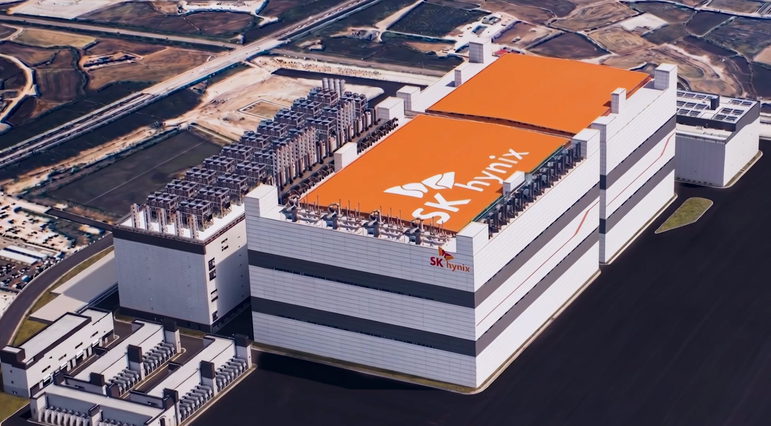
Massive $870B investment in AI hardware and memory will reshape the global supply chain for AI infrastructure.
30-Second TL;DR
What Changed
Total investment of 1.35 quadrillion KRW (~$870 billion) over 10 years
Why It Matters
This massive capital injection will significantly increase the supply of high-bandwidth memory (HBM) and advanced chips, which are critical bottlenecks for current AI model training and inference.
What To Do Next
Monitor HBM supply availability and pricing trends as these will directly impact the cost and scalability of your AI infrastructure deployments.
Key Points
- •Total investment of 1.35 quadrillion KRW (~$870 billion) over 10 years
- •Focus on advanced wafer fabrication and AI-specific memory production
- •Strategic effort to secure dominance in the global AI hardware supply chain
Deep Insight
AI-generated analysis for this event — not the original article.
Enhanced Key Takeaways
- •The investment is part of the South Korean government's 'K-Semiconductor Belt' initiative, which aims to create the world's largest semiconductor cluster in the Gyeonggi province.
- •A significant portion of the funding is earmarked for the development of next-generation High Bandwidth Memory (HBM4 and HBM4E) to meet the surging demand from AI accelerator manufacturers like NVIDIA.
- •The plan includes the construction of multiple 'Mega Fabs' that will utilize advanced EUV (Extreme Ultraviolet) lithography technology to shrink process nodes below 2nm.
- •The initiative addresses critical supply chain vulnerabilities by fostering a domestic ecosystem for semiconductor materials, components, and equipment (MCE) to reduce reliance on foreign imports.
- •The project involves a public-private partnership model where the government provides tax incentives and infrastructure support, such as power and water supply, to offset the massive capital expenditure.
Competitor Analysis
- Samsung/SK Hynix (Korea)
- Memory (HBM) & Logic Foundry
- TSMC (Taiwan)
- Advanced Logic Foundry
- Intel (USA)
- IDM 2.0 (Foundry + Design)
- Samsung/SK Hynix (Korea)
- 2nm / 1.4nm roadmap
- TSMC (Taiwan)
- 2nm / 1.6nm (A16)
- Intel (USA)
- 18A / 14A nodes
- Samsung/SK Hynix (Korea)
- Memory-centric AI hardware
- TSMC (Taiwan)
- Compute-centric (CoWoS packaging)
- Intel (USA)
- Integrated AI PC & Data Center
- Samsung/SK Hynix (Korea)
- Massive tax credits/infrastructure
- TSMC (Taiwan)
- Strategic subsidies (CHIPS Act)
- Intel (USA)
- CHIPS Act grants/loans
| Feature | Samsung/SK Hynix (Korea) | TSMC (Taiwan) | Intel (USA) |
|---|---|---|---|
| Primary Focus | Memory (HBM) & Logic Foundry | Advanced Logic Foundry | IDM 2.0 (Foundry + Design) |
| Process Node | 2nm / 1.4nm roadmap | 2nm / 1.6nm (A16) | 18A / 14A nodes |
| AI Strategy | Memory-centric AI hardware | Compute-centric (CoWoS packaging) | Integrated AI PC & Data Center |
| Govt Support | Massive tax credits/infrastructure | Strategic subsidies (CHIPS Act) | CHIPS Act grants/loans |
Technical Deep Dive
- Focus on HBM4 integration: Moving to 12-high and 16-high stacks to increase memory bandwidth and capacity for large language model (LLM) training.
- Advanced Packaging: Expansion of 2.5D and 3D packaging capabilities (such as Samsung's I-Cube and SK Hynix's advanced MR-MUF) to improve thermal management and signal integrity.
- EUV Lithography: Deployment of high-NA EUV scanners to enable sub-2nm fabrication, critical for high-performance AI logic chips.
- Power Efficiency: Implementation of backside power delivery networks (BSPDN) to reduce voltage drop and improve performance in AI-specific logic circuits.
Future ImplicationsAI analysis grounded in cited sources
Timeline
- 2023-03South Korean government announces the 'K-Semiconductor Belt' strategy to attract private investment.
- 2024-01Samsung and SK Hynix commit to initial phases of the mega-cluster project in Yongin.
- 2025-05Government confirms tax incentives and infrastructure acceleration for the 10-year semiconductor plan.
- 2026-02Samsung begins pilot production of advanced HBM3E/HBM4 prototypes for AI partners.
Weekly AI Recap
Read this week's curated digest of top AI events →
Related Updates
AI-curated news aggregator. All content rights belong to original publishers.
Original source: cnBeta (Full RSS) ↗
This is a summary, not the original. Read the source, or get the weekly briefing.
The weekly digest
One email a week. Unsubscribe anytime.