Researchers achieve 3D vertical silicon chip stacking
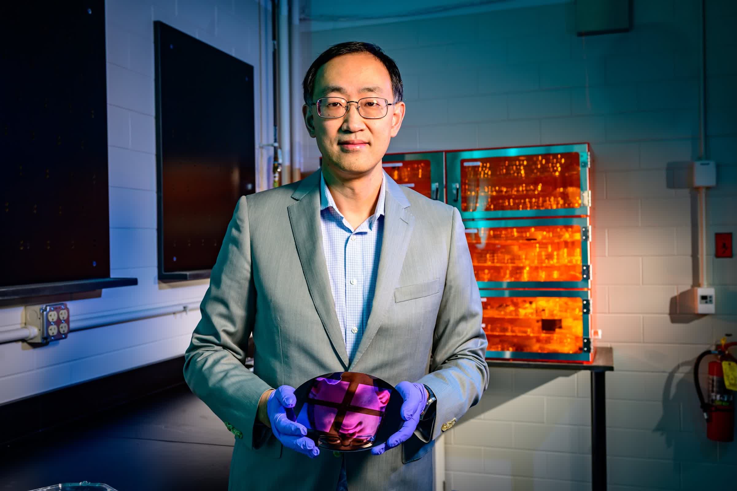
💡A breakthrough in 3D chip stacking could be the key to overcoming current hardware bottlenecks for AI compute.
⚡ 30-Second TL;DR
What Changed
Successfully stacked three active silicon layers on a single chip
Why It Matters
This research could significantly accelerate the development of high-density AI accelerators by enabling more transistors in a smaller footprint.
What To Do Next
Follow the research progress from UIUC to anticipate future hardware constraints for large-scale model training.
Key Points
- •Successfully stacked three active silicon layers on a single chip
- •Achieved 98% to 100% transistor yield in vertical configuration
- •Provides a viable path for scaling compute density beyond traditional planar limits
🧠 Deep Insight
Background and context from public sources — not the original article. 12 sources cited.
🔑 Enhanced Key Takeaways
- •The University of Illinois Urbana-Champaign (UIUC) team, led by Professor Qing Cao, developed a low-temperature manufacturing process using ultra-thin freestanding silicon nanomembranes transferred onto a receiving substrate via a roll laminator.
- •The bonding process for stacking layers operates at temperatures no higher than 200 degrees Celsius, which is significantly lower than the approximately 1,000 degrees Celsius typically required for high-quality crystalline silicon fabrication, thereby preventing damage to existing metal interconnects in lower layers.
- •This breakthrough represents true monolithic 3D integration, where each active device layer is sequentially built directly on top of the previous one during fabrication, enabling 10 to 100 times denser interlayer vertical connections and nanometer-scale alignment, in contrast to conventional 3D packaging methods that bond pre-fabricated dies.
- •The stacked layers utilize "junctionless" transistors, where the silicon is heavily and uniformly doped before stacking, eliminating the need for high-temperature doping steps after each layer is formed.
- •The research was conducted through Illinois Grainger Engineering's Center for Advanced Semiconductor Chips with Accelerated Performance (ASAP), with significant industry backing from partners including IBM, Intel, and Taiwan Semiconductor Manufacturing Company (TSMC).
🛠️ Technical Deep Dive
- Integration Method: Monolithic 3D integration, where device layers are built sequentially on top of each other.
- Material: Utilizes standard single-crystalline silicon.
- Layer Transfer: Ultra-thin freestanding silicon nanomembranes are created from a donor wafer and transferred using a roll laminator onto a receiving substrate with completed circuitry.
- Thermal Budget: The bonding process for stacking layers requires temperatures of no more than 200 degrees Celsius, which is crucial for preserving underlying metal interconnects.
- Transistor Design: Employs junctionless transistors, where the silicon is heavily and uniformly doped prior to stacking, avoiding high-temperature post-fabrication doping.
- Interconnects: Layers are connected using vertical metal interconnects.
- Yield: Achieved 98% to 100% transistor yield for three stacked active silicon layers, each containing 625 transistors, even in an academic laboratory setting.
- Performance: Output current densities of the stacked transistors matched those of conventional silicon transistors fabricated on bulk wafers at much higher temperatures and outperformed monolithic devices made from alternative materials by at least a factor of three to four.
🔮 Future ImplicationsAI analysis grounded in cited sources
⏳ Timeline
📎 Sources (12)
Factual claims are grounded in the sources below. Forward-looking analysis is AI-generated interpretation.
Weekly AI Recap
Read this week's curated digest of top AI events →
👉Related Updates
AI-curated news aggregator. All content rights belong to original publishers.
Original source: cnBeta (Full RSS) ↗
This is a summary, not the original. Read the source, or get the weekly briefing.
The weekly digest
One email a week. Unsubscribe anytime.