來源cnBeta (Full RSS)•較早收集於 2h
研究團隊實現矽晶片垂直堆疊技術
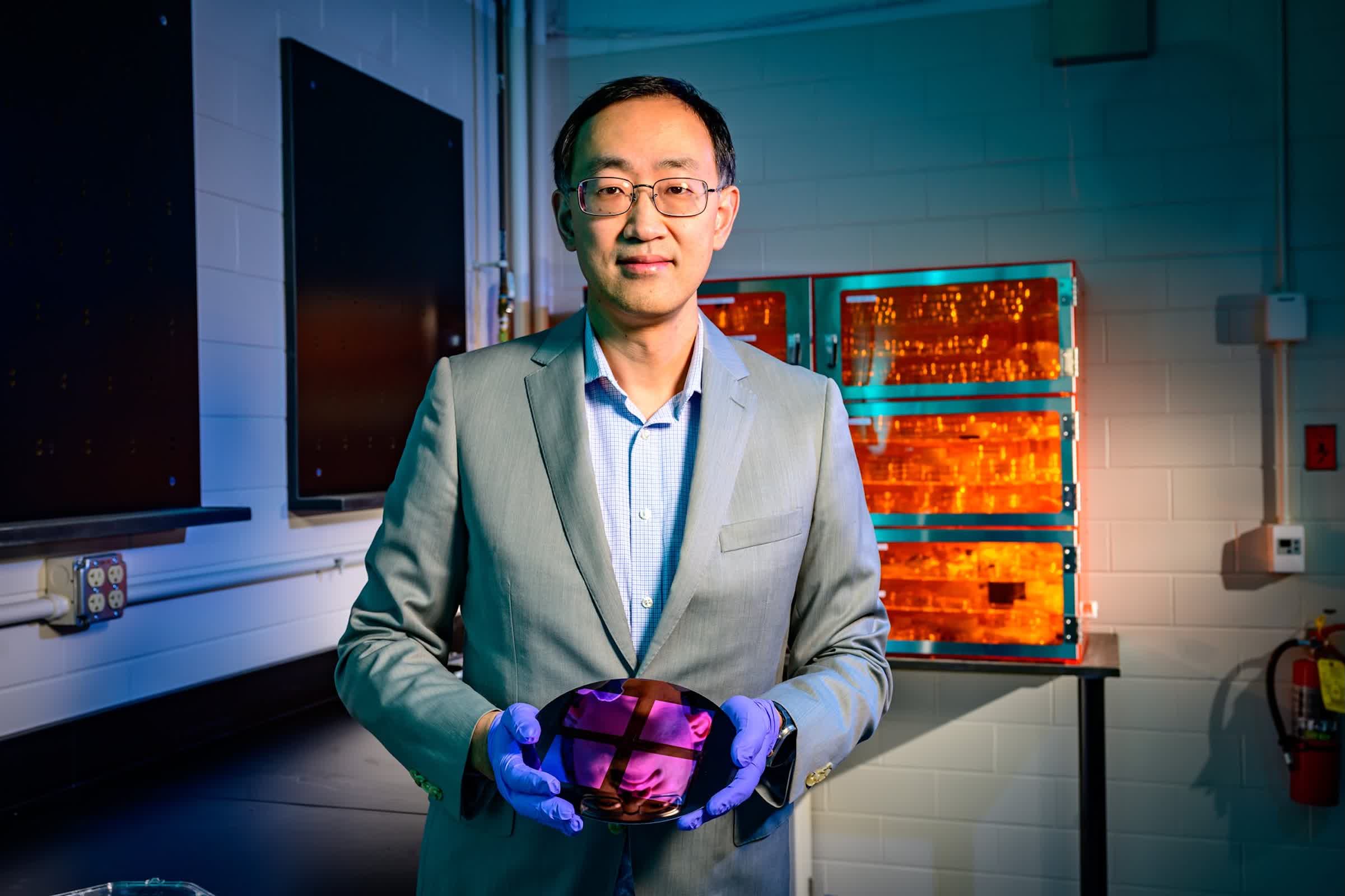
#semiconductor#moores-law#hardware-innovationvertical-3d-silicon-stackinguniversity of illinois urbana-champaign
💡3D 晶片堆疊的突破可能是克服當前 AI 算力硬體瓶頸的關鍵。
⚡ 30 秒速覽
有什麼變化
成功在單一晶片上垂直堆疊三層有源矽電路
為什麼重要
這項研究透過在更小的空間內容納更多晶體管,可能顯著加速高密度 AI 加速器的開發。
下一步行動
追蹤 UIUC 的研究進展,以預判未來大規模模型訓練的硬體限制。
誰應關注:Researchers & Academics
關鍵要點
- •成功在單一晶片上垂直堆疊三層有源矽電路
- •在垂直配置中實現了 98% 至 100% 的晶體管良率
- •為超越傳統平面限制的算力密度擴展提供了可行路徑
🧠 深度解析
背景與延伸:來自公開資料,非原文內容。引用 12 個來源。
🔑 增強重點摘要
- •The University of Illinois Urbana-Champaign (UIUC) team, led by Professor Qing Cao, developed a low-temperature manufacturing process using ultra-thin freestanding silicon nanomembranes transferred onto a receiving substrate via a roll laminator.
- •The bonding process for stacking layers operates at temperatures no higher than 200 degrees Celsius, which is significantly lower than the approximately 1,000 degrees Celsius typically required for high-quality crystalline silicon fabrication, thereby preventing damage to existing metal interconnects in lower layers.
- •This breakthrough represents true monolithic 3D integration, where each active device layer is sequentially built directly on top of the previous one during fabrication, enabling 10 to 100 times denser interlayer vertical connections and nanometer-scale alignment, in contrast to conventional 3D packaging methods that bond pre-fabricated dies.
- •The stacked layers utilize "junctionless" transistors, where the silicon is heavily and uniformly doped before stacking, eliminating the need for high-temperature doping steps after each layer is formed.
- •The research was conducted through Illinois Grainger Engineering's Center for Advanced Semiconductor Chips with Accelerated Performance (ASAP), with significant industry backing from partners including IBM, Intel, and Taiwan Semiconductor Manufacturing Company (TSMC).
🛠️ 技術深入
- Integration Method: Monolithic 3D integration, where device layers are built sequentially on top of each other.
- Material: Utilizes standard single-crystalline silicon.
- Layer Transfer: Ultra-thin freestanding silicon nanomembranes are created from a donor wafer and transferred using a roll laminator onto a receiving substrate with completed circuitry.
- Thermal Budget: The bonding process for stacking layers requires temperatures of no more than 200 degrees Celsius, which is crucial for preserving underlying metal interconnects.
- Transistor Design: Employs junctionless transistors, where the silicon is heavily and uniformly doped prior to stacking, avoiding high-temperature post-fabrication doping.
- Interconnects: Layers are connected using vertical metal interconnects.
- Yield: Achieved 98% to 100% transistor yield for three stacked active silicon layers, each containing 625 transistors, even in an academic laboratory setting.
- Performance: Output current densities of the stacked transistors matched those of conventional silicon transistors fabricated on bulk wafers at much higher temperatures and outperformed monolithic devices made from alternative materials by at least a factor of three to four.
🔮 前景展望基於引用來源的 AI 分析
This monolithic 3D integration technique could significantly extend Moore's Law.
By building upward with high-density vertical connections, it allows for increased transistor density and computing power without further shrinking individual transistors, addressing physical limits of 2D scaling.
The technology could enable more energy-efficient computing, particularly for AI and data-intensive applications.
Shorter interconnect distances between stacked layers reduce parasitic capacitance, decrease signal propagation delay, and lower power consumption.
Commercial adoption of this monolithic 3D integration method is plausible within years.
The research was conducted with industry partners (IBM, Intel, TSMC) through the NSF ASAP center, and the team is actively preparing for transfer to a commercial foundry, indicating a path to production.
⏳ 時間線
1960-02
Jim Early of Bell Labs publicly discusses stacking components in a 3D cubic arrangement at the ISSCC.
1983-XX
Hitachi files a Japanese patent for 3D IC stacked chips using through-silicon vias (TSVs).
2007-09
Hynix introduces 24-layer 3D IC technology for NAND flash memory.
2011-10
Samsung and Micron Technology announce TSV-based Hybrid Memory Cube (HMC) technology.
2022-XX
AMD introduces Zen 4 processors, some featuring 3D V-Cache utilizing 3D stacking.
2026-05
University of Illinois Urbana-Champaign researchers achieve high-yield 3D vertical silicon chip stacking using a low-temperature monolithic integration method.
📎 來源 (12)
Factual claims are grounded in the sources below. Forward-looking analysis is AI-generated interpretation.
📰
AI 週報
閱讀本週精選 AI 大事摘要 →
👉相關動態
AI 策展新聞聚合。所有內容版權歸原始發布者所有。
原始來源: cnBeta (Full RSS) ↗
每週電子報
每週一封,可隨時退訂。