Prinano validates mass production of optical chips without DUV
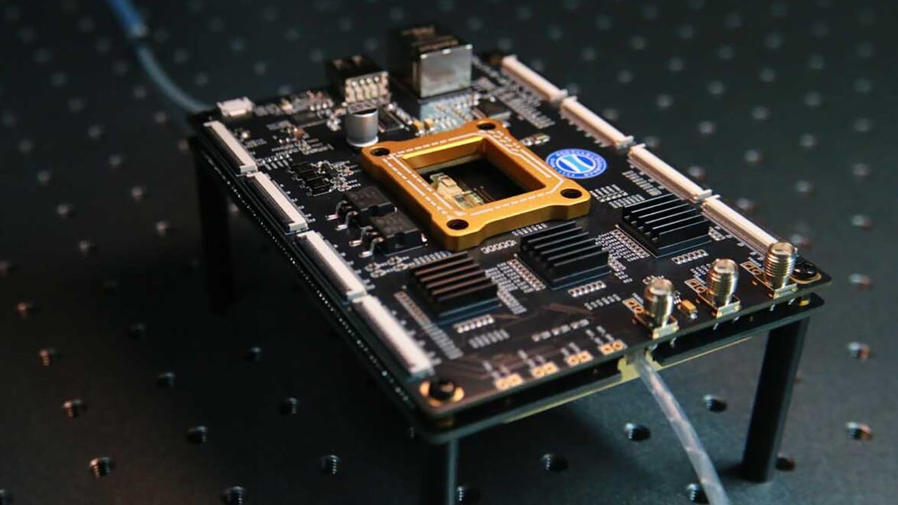
💡A potential game-changer for AI hardware infrastructure by slashing chip manufacturing costs without DUV gear.
⚡ 30-Second TL;DR
What Changed
Prinano validated mass production of 8-inch photonic wafers
Why It Matters
This breakthrough could significantly lower the barrier for manufacturing high-speed optical interconnects, which are critical for scaling AI data center infrastructure.
What To Do Next
Monitor the availability of photonic chip prototyping services to prepare for potential integration into next-gen AI hardware.
Key Points
- •Prinano validated mass production of 8-inch photonic wafers
- •Technology avoids DUV lithography entirely
- •Production costs reduced to one-tenth of conventional methods
🧠 Deep Insight
Background and context from public sources — not the original article. 21 sources cited.
🔑 Enhanced Key Takeaways
- •Prinano's PL-SR series utilizes an inkjet step-and-repeat nanoimprint lithography (NIL) system for patterning.
- •The company's technology has demonstrated sub-10nm linewidth capability, which reportedly surpasses the 14nm linewidth achieved by Canon's FPA-1200NZ2C NIL machine.
- •Prinano's nanoimprint system is particularly well-suited for manufacturing memory chips (such as NAND flash), silicon-based microdisplays, silicon photonics, and advanced packaging applications, rather than complex logic chips.
- •A proprietary template profile control mechanism is integrated into Prinano's system to compensate for curvature mismatches between the rigid quartz mold and the silicon wafer, enabling the transfer of features with aspect ratios over 7:1 without distortion.
- •Prinano is recognized as the second company globally, following Canon, to successfully deliver a semiconductor-grade nanoimprint lithography tool to a customer for actual chip production.
📊 Competitor Analysis▸ Show
| Feature/Company | Prinano (PL-SR Series) | Canon (FPA-1200NZ2C) |
|---|---|---|
| Technology Type | Inkjet Step-and-Repeat Nanoimprint Lithography | Nanoimprint Lithography (NIL) |
| Linewidth Capability | Less than 10nm | 14nm (claimed 5nm process capability) |
| Target Applications | NAND Flash, memory chips, silicon-based microdisplays, silicon photonics, advanced packaging | 5nm-class process technology, high-end research, memory, photonics |
| Wafer Size | 300mm (12-inch) wafers | Not explicitly stated for FPA-1200NZ2C, but NIL generally supports various sizes. |
| Cost (Tool) | Not disclosed, but NIL is generally a fraction of DUV/EUV costs | Approximately $15 million (compared to >$150 million for EUV) |
| Delivery Status | First semiconductor-grade tool delivered to a Chinese customer in August 2025 | First commercial NIL machine delivered to Texas Institute for Electronics in 2024 |
🛠️ Technical Deep Dive
- Prinano's PL-SR system patterns wafers by physically pressing a rigid quartz mold, engraved with nanoscale circuit designs, into a thin layer of liquid resist on the wafer surface.
- It utilizes a high-precision inkjet system to apply the resist, dynamically adjusting droplet volume based on pattern densities to ensure a thin and uniform residual layer, typically under 10nm on average with less than 2nm variation.
- The system is capable of processing 300mm (12-inch) wafers and achieves linewidths below 10nm.
- A proprietary template profile control mechanism is employed to compensate for curvature mismatches between the quartz mold and the silicon wafer, facilitating the transfer of features with aspect ratios exceeding 7:1 without distortion.
- The process involves precise alignment of the mold and wafer, making full contact without a vacuum, and imprinting each field sequentially (step-and-repeat) to cover the entire wafer.
- Prinano has developed multiple UV-curable resist systems, including solvent-developable options, compatible with inkjet step-and-repeat processes to prevent template contamination.
🔮 Future ImplicationsAI analysis grounded in cited sources
⏳ Timeline
📎 Sources (21)
Factual claims are grounded in the sources below. Forward-looking analysis is AI-generated interpretation.
Weekly AI Recap
Read this week's curated digest of top AI events →
👉Related Updates

AI-curated news aggregator. All content rights belong to original publishers.
Original source: SCMP Technology ↗
This is a summary, not the original. Read the source, or get the weekly briefing.
The weekly digest
One email a week. Unsubscribe anytime.