Micron Bets $10B on Post-Memory Research
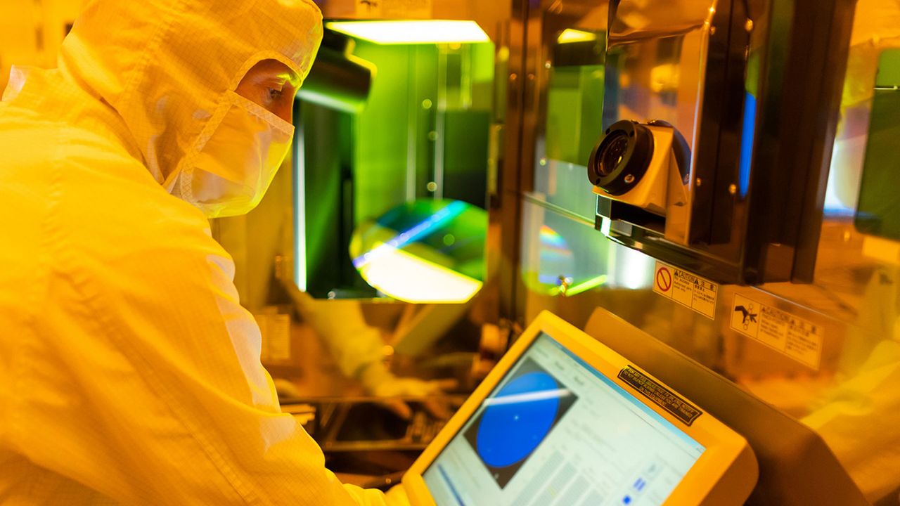
💡A $10B memory bet could reshape the bandwidth and packaging roadmap behind future AI accelerators.
⚡ 30-Second TL;DR
What Changed
Micron is committing $10 billion to U.S.-based research facilities.
Why It Matters
The investment could strengthen the U.S. memory technology ecosystem and create longer-term alternatives to current memory architectures. For AI infrastructure, advances in memory and packaging may eventually improve bandwidth, capacity, and energy efficiency for large-scale accelerators.
What To Do Next
Track Micron Research Labs announcements and evaluate whether future memory or packaging advances could change your accelerator bandwidth and capacity assumptions.
Key Points
- •Micron is committing $10 billion to U.S.-based research facilities.
- •The Boise hub will target technologies beyond conventional DRAM and NAND.
- •Research will cover next-generation memory and advanced packaging.
- •The program will coordinate work across industry, academia, startups, and government.
🧠 Deep Insight
Background and context from public sources — not the original article. 9 sources cited.
🔑 Enhanced Key Takeaways
- •The $10 billion investment is structured to be deployed over a 10-year period, rather than as a single immediate capital expenditure.
- •The Boise research hub is part of a significantly larger, long-term commitment by Micron to invest over $250 billion in U.S.-based manufacturing, research, and development.
- •Micron CEO Sanjay Mehrotra has explicitly positioned memory as critical 'strategic infrastructure' for AI, arguing that current memory bottlenecks prevent AI models from scaling effectively.
- •The facility is slated to break ground in calendar year 2027, serving as a physical venue for industry-wide innovation forums and research conferences.
- •The initiative is specifically designed to help Micron close the competitive gap with major rivals Samsung Electronics and SK Hynix in the high-growth AI memory sector.
📊 Competitor Analysis▸ Show
| Feature | Micron (Research Labs) | Samsung Electronics | SK Hynix |
|---|---|---|---|
| AI Memory Focus | Post-DRAM/NAND & Packaging | HBM3E/HBM4 & CXL | HBM3E/HBM4 & PIM |
| R&D Strategy | Collaborative Boise Hub | Vertical Integration | Specialized AI Memory |
| Market Position | Challenger in AI Memory | Market Leader | HBM Market Leader |
🛠️ Technical Deep Dive
- Focus on post-DRAM and post-NAND architectures to address memory wall limitations in AI compute.
- Development of advanced semiconductor packaging techniques to improve bandwidth and power efficiency.
- Research into next-generation compute-in-memory (CIM) and memory-centric architectures.
- Exploration of future manufacturing processes to support high-density, low-latency memory requirements.
🔮 Future ImplicationsAI analysis grounded in cited sources
⏳ Timeline
📎 Sources (9)
Factual claims are grounded in the sources below. Forward-looking analysis is AI-generated interpretation.
Weekly AI Recap
Read this week's curated digest of top AI events →
👉Related Updates
AI-curated news aggregator. All content rights belong to original publishers.
Original source: Tom's Hardware ↗
This is a summary, not the original. Read the source, or get the weekly briefing.
Weekly AI briefing
One email a week. Unsubscribe anytime.