Intel May Bring bLLC to Razor Lake Mobile Chips
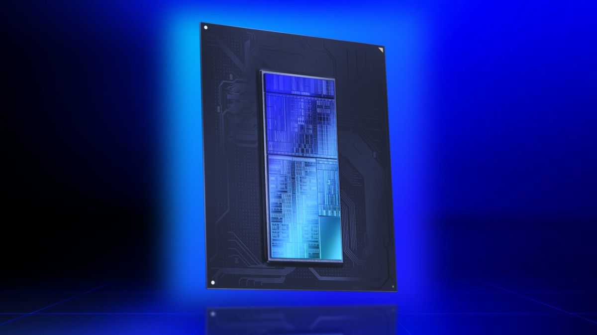
💡A rumored Intel cache strategy could change latency and efficiency expectations for future CPU-based AI workloads.
⚡ 30-Second TL;DR
What Changed
Nova Lake desktop CPUs may be the first and only initial recipients of Intel bLLC.
Why It Matters
If the rumor is accurate, Intel could use larger cache to improve latency-sensitive workloads and gaming performance across premium CPUs. For AI practitioners, the main relevance is potential platform-level performance and power differences, but the claims remain unverified.
What To Do Next
Track Intel’s official Nova Lake and Razor Lake disclosures before committing new AI inference servers to a cache-sensitive CPU platform.
Key Points
- •Nova Lake desktop CPUs may be the first and only initial recipients of Intel bLLC.
- •Razor Lake-HX could introduce bLLC to Intel’s mobile lineup.
- •Razor Lake-AX is also a possible bLLC target, according to the leak.
- •The Razor Lake family is rumored to use TSMC’s N2X process node.
🧠 Deep Insight
AI-generated analysis for this event.
🔑 Enhanced Key Takeaways
- •bLLC (big Last Level Cache) is Intel's strategic response to AMD's 3D V-Cache technology, aiming to mitigate latency issues in high-performance computing workloads.
- •The transition to TSMC's N2X process node represents a significant shift in Intel's manufacturing strategy, prioritizing high-performance logic density for its next-generation mobile architectures.
- •Industry analysts suggest that the implementation of bLLC in mobile chips will require advanced packaging solutions, likely utilizing Foveros technology to manage thermal constraints.
- •Razor Lake-HX is expected to target the enthusiast mobile segment, positioning Intel to compete directly with AMD's high-end mobile processors that utilize stacked cache.
- •The integration of bLLC is part of a broader Intel roadmap to improve IPC (Instructions Per Clock) gains without relying solely on frequency scaling, which has hit thermal walls in mobile form factors.
📊 Competitor Analysis▸ Show
| Feature | Intel bLLC (Razor Lake) | AMD 3D V-Cache (X3D) | Apple Silicon (M-Series) |
|---|---|---|---|
| Architecture | Hybrid (P+E Cores) + bLLC | Chiplet (Zen) + 3D Stacked SRAM | Unified Memory Architecture |
| Manufacturing | TSMC N2X | TSMC N4/N3 | TSMC N3/N2 |
| Primary Benefit | Latency reduction for gaming/compute | Massive L3 cache for gaming | Memory bandwidth & efficiency |
🛠️ Technical Deep Dive
- bLLC Implementation: Utilizes a dedicated SRAM die stacked directly onto the compute die to increase L3 cache capacity significantly beyond standard on-die limits.
- TSMC N2X Node: Optimized for high-performance computing, offering improved power efficiency and transistor density compared to N3P, specifically targeting high-frequency operation.
- Packaging: Expected to leverage Intel's Foveros 3D packaging technology to enable high-bandwidth, low-latency interconnects between the compute tiles and the cache die.
- Thermal Management: The use of bLLC in mobile chips necessitates sophisticated power delivery and thermal throttling algorithms to prevent localized hotspots on the stacked die.
🔮 Future ImplicationsAI analysis grounded in cited sources
⏳ Timeline
Weekly AI Recap
Read this week's curated digest of top AI events →
👉Related Updates


AI-curated news aggregator. All content rights belong to original publishers.
Original source: Tom's Hardware ↗