Huawei unveils 1.4nm chip roadmap via new scaling law
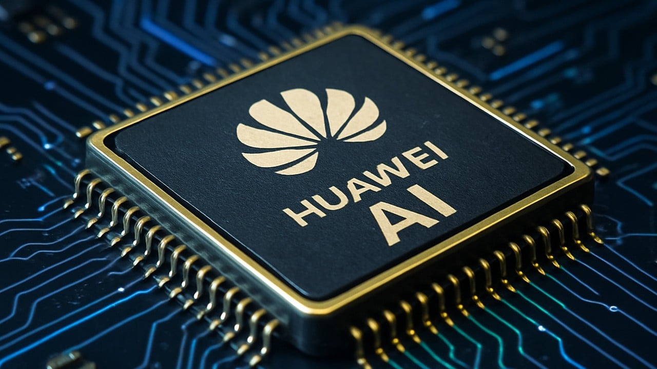
Understand how Huawei's new scaling law could reshape the future of AI hardware and semiconductor self-reliance.
30-Second TL;DR
What Changed
Introduction of the Tau (τ) Scaling Law to guide future chip architecture.
Why It Matters
This development signals a long-term shift in AI hardware availability, potentially reducing reliance on Western lithography equipment. It suggests that future high-performance AI compute could be sustained through domestic Chinese innovation.
What To Do Next
Monitor Huawei's hardware releases and whitepapers on the Tau Scaling Law to assess potential shifts in AI training infrastructure requirements.
Key Points
- •Introduction of the Tau (τ) Scaling Law to guide future chip architecture.
- •Targeting 1.4nm equivalent process node performance by 2031.
- •Strategic focus on achieving semiconductor self-reliance for Huawei's hardware ecosystem.
Deep Insight
Background and context from public sources — not the original article. 12 sources cited.
Enhanced Key Takeaways
- •The Tau (τ) Scaling Law, also dubbed "He's Law" by peers, proposes a paradigm shift that replaces the traditional geometric miniaturization of transistors with time (τ) scaling as a guiding principle for semiconductor and electronic system evolution.
- •Based on the Tau Scaling Law, Huawei has developed an innovative core technology called LogicFolding architecture, designed to reduce the resistive and capacitive load of signal propagation, thereby boosting transistor density.
- •Huawei claims to have utilized the Tau Scaling Law to design and mass produce 381 chips over the past six years, indicating a long-term application of this new architectural principle.
- •The company's target of achieving 1.4nm equivalent process node performance by 2031 is particularly significant as it aims to defy the industry consensus that state-of-the-art extreme ultraviolet (EUV) lithography machines, primarily from ASML, are necessary for manufacturing chips at such advanced nodes.
- •Huawei's semiconductor chief, He Tingbo, presented the Tau Scaling Law at the 2026 IEEE International Symposium on Circuits and Systems (ISCAS) in Shanghai, highlighting its importance to the company's future strategy.
Competitor Analysis
- Process Node
- 1.4nm equivalent
- Target Mass Production
- 2031
- Key Technologies/Notes
- Tau (τ) Scaling Law, LogicFolding architecture; aims to achieve without cutting-edge EUV lithography.
- Process Node
- A14 (1.4nm)
- Target Mass Production
- H2 2028
- Key Technologies/Notes
- Successor to N2 platform, 15% higher performance or 30% lower power, 20% logic density increase; NanoFlex Pro nanosheet transistor architecture; uses 0.33 NA EUV lithography.
- Process Node
- SF1.4 (1.4nm)
- Target Mass Production
- 2029 (revised from 2027)
- Key Technologies/Notes
- Optimized for consumer/smartphone applications; may feature new GAA transistor design; will not feature backside power delivery.
- Process Node
- 14A (1.4nm)
- Target Mass Production
- 2029
- Key Technologies/Notes
- Introduces 2nd Gen RibbonFET GAA transistors, revamped PowerDirect backside power delivery, and Turbo Cells; expected to be the first to adopt High-NA EUV lithography for volume manufacturing.
| Company | Process Node | Target Mass Production | Key Technologies/Notes |
|---|---|---|---|
| Huawei | 1.4nm equivalent | 2031 | Tau (τ) Scaling Law, LogicFolding architecture; aims to achieve without cutting-edge EUV lithography. |
| TSMC | A14 (1.4nm) | H2 2028 | Successor to N2 platform, 15% higher performance or 30% lower power, 20% logic density increase; NanoFlex Pro nanosheet transistor architecture; uses 0.33 NA EUV lithography. |
| Samsung | SF1.4 (1.4nm) | 2029 (revised from 2027) | Optimized for consumer/smartphone applications; may feature new GAA transistor design; will not feature backside power delivery. |
| Intel | 14A (1.4nm) | 2029 | Introduces 2nd Gen RibbonFET GAA transistors, revamped PowerDirect backside power delivery, and Turbo Cells; expected to be the first to adopt High-NA EUV lithography for volume manufacturing. |
Technical Deep Dive
- The Tau (τ) Scaling Law proposes a shift from traditional geometric scaling of transistors to time (τ) scaling as a guiding principle for semiconductor and electronic system evolution.
- Based on this law, Huawei has developed the LogicFolding architecture, which aims to reduce the resistive and capacitive load of signal propagation, thereby increasing transistor density.
- The approach involves a multi-level co-optimization mechanism across semiconductor devices, circuits, chips, and systems to systematically shorten the time constant τ.
- At the device level, this includes optimizing the resistance and parasitic capacitance of transistors and interconnects.
- At the chip level, it involves full-stack coordinated design of software, architecture, and silicon to achieve fine-grained, workload-driven control over instruction and data flows, enhancing system-level parallelism and efficiency.
- At the system level, the law guides redefining interconnect protocols with UnifiedBus to achieve unified memory addressing and native memory semantics for SuperPoDs, significantly reducing system communications latency.
- Huawei has also previously utilized Self-Aligned Quadruple Patterning (SAQP) technology as a method to increase transistor density without relying on advanced EUV lithography tools, which are restricted from reaching China.
Future ImplicationsAI analysis grounded in cited sources
Timeline
- 1991Huawei's ASIC design center (later HiSilicon) was founded.
- 2004-10Shenzhen HiSilicon Semiconductor Co., Ltd. was formally established as an independent entity.
- 2019-05US Department of Commerce added Huawei to its Entity List, restricting access to US technology.
- 2020-09-15Huawei announced it would stop producing its Kirin chipsets due to US sanctions impacting its supply chain.
- 2023-08-29Huawei announced the first fully domestically fabricated chip, the Kirin 9000S, for its Mate 60 Pro series.
- 2026-05-25Huawei unveils the Tau (τ) Scaling Law and LogicFolding architecture, targeting 1.4nm equivalent chips by 2031.
Sources (12)
Factual claims are grounded in the sources below. Forward-looking analysis is AI-generated interpretation.
Weekly AI Recap
Read this week's curated digest of top AI events →
Related Updates


AI-curated news aggregator. All content rights belong to original publishers.
Original source: SCMP Technology ↗
This is a summary, not the original. Read the source, or get the weekly briefing.
The weekly digest
One email a week. Unsubscribe anytime.