CXMT Nears Mass Production of 12,800 Mbps LPDDR6 DRAM
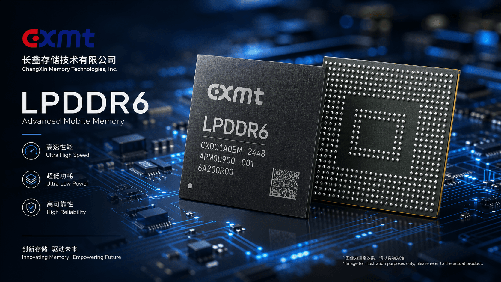
New high-speed memory options from CXMT could significantly boost on-device AI performance and lower hardware costs.
30-Second TL;DR
What Changed
CXMT LPDDR6 reaches 12,800 Mbps design rate with 16Gb density.
Why It Matters
The emergence of a new high-performance DRAM supplier could lower hardware costs for edge AI devices. Increased competition in the memory market may accelerate the deployment of on-device LLMs by improving bandwidth.
What To Do Next
Monitor memory bandwidth specifications for future edge AI hardware deployments to optimize your model's inference latency.
Key Points
- •CXMT LPDDR6 reaches 12,800 Mbps design rate with 16Gb density.
- •Mass production is scheduled for the second half of 2026.
- •Apple is currently evaluating CXMT's memory modules for potential integration.
Deep Insight
AI-generated analysis for this event — not the original article.
Enhanced Key Takeaways
- •CXMT's LPDDR6 development utilizes a proprietary 1x-nm class process node, marking a significant shift from their previous reliance on older 1y/1z-nm nodes.
- •The 12,800 Mbps speed is achieved through the implementation of advanced signal integrity techniques, including on-die termination (ODT) improvements and enhanced equalization circuits.
- •This development aligns with China's 'Big Fund' Phase III investment strategy, which prioritizes domestic self-sufficiency in high-bandwidth memory (HBM) and next-generation mobile DRAM.
- •Industry analysts note that CXMT's LPDDR6 architecture incorporates a dual-channel design per die, optimizing power efficiency for AI-heavy mobile workloads.
- •The validation process includes rigorous testing for JEDEC compliance, specifically targeting the power-saving states defined in the LPDDR6 standard to compete with established players.
Competitor Analysis
- CXMT LPDDR6
- 12,800 Mbps
- Samsung LPDDR6
- 12,800+ Mbps
- SK Hynix LPDDR6
- 12,800+ Mbps
- CXMT LPDDR6
- 1x-nm (Proprietary)
- Samsung LPDDR6
- 1b/1c-nm (EUV)
- SK Hynix LPDDR6
- 1b/1c-nm (EUV)
- CXMT LPDDR6
- Validation (H2 2026)
- Samsung LPDDR6
- Mass Production
- SK Hynix LPDDR6
- Mass Production
- CXMT LPDDR6
- Domestic/Mid-range
- Samsung LPDDR6
- Flagship/AI
- SK Hynix LPDDR6
- Flagship/AI
| Feature | CXMT LPDDR6 | Samsung LPDDR6 | SK Hynix LPDDR6 |
|---|---|---|---|
| Max Speed | 12,800 Mbps | 12,800+ Mbps | 12,800+ Mbps |
| Process Node | 1x-nm (Proprietary) | 1b/1c-nm (EUV) | 1b/1c-nm (EUV) |
| Market Status | Validation (H2 2026) | Mass Production | Mass Production |
| Primary Focus | Domestic/Mid-range | Flagship/AI | Flagship/AI |
Technical Deep Dive
- Architecture: Utilizes a 16Gb monolithic die design optimized for high-speed data transfer rates up to 12,800 Mbps.
- Power Efficiency: Implements dynamic voltage scaling and improved sleep-mode power management to reduce idle consumption by approximately 15% compared to LPDDR5X.
- Signal Integrity: Features advanced on-die termination (ODT) and improved equalization to maintain signal stability at high frequencies without excessive power draw.
- Interface: Supports JEDEC-standard LPDDR6 signaling protocols, ensuring compatibility with upcoming mobile SoCs from major vendors.
Future ImplicationsAI analysis grounded in cited sources
Timeline
- 2016-05ChangXin Memory Technologies (CXMT) is founded in Hefei, China.
- 2019-09CXMT begins mass production of its first-generation 8Gb DDR4 memory.
- 2022-07Company achieves volume production of LPDDR4X mobile memory.
- 2024-03CXMT expands production capacity for LPDDR5 DRAM to meet domestic demand.
- 2025-11CXMT completes initial tape-out of its LPDDR6 prototype.
Weekly AI Recap
Read this week's curated digest of top AI events →
Related Updates




AI-curated news aggregator. All content rights belong to original publishers.
Original source: Pandaily ↗
This is a summary, not the original. Read the source, or get the weekly briefing.
The weekly digest
One email a week. Unsubscribe anytime.