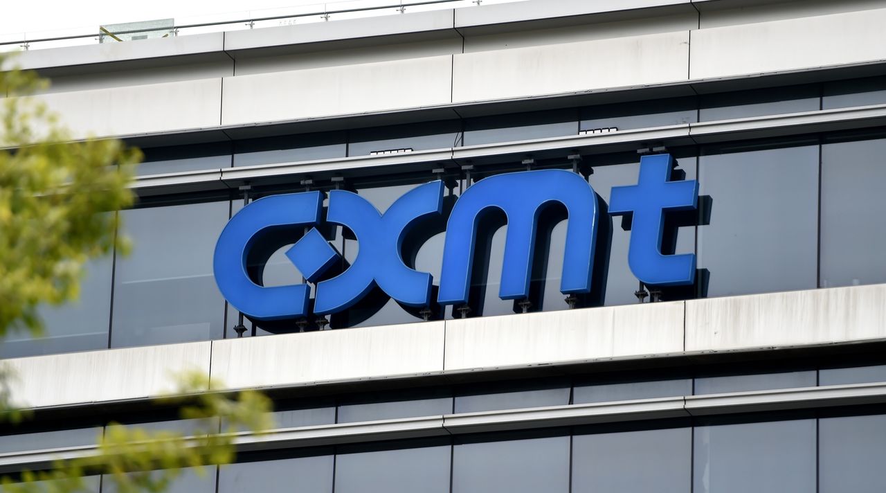
Court Hears CXMT Used Stolen Samsung DRAM IP
💡A semiconductor IP case could reshape memory sourcing and compliance for AI server builders.
⚡ 30-Second TL;DR
What Changed
The alleged theft involves Samsung’s process recipes for an 18nm-class DRAM node.
Why It Matters
If proven, the allegations could intensify scrutiny of Chinese memory suppliers and increase restrictions around semiconductor technology transfers. AI companies may also face greater diligence requirements when sourcing DRAM and other critical components.
What To Do Next
Audit your memory suppliers’ provenance records and require documented IP-compliance attestations before qualifying DRAM for AI servers.
Key Points
- •The alleged theft involves Samsung’s process recipes for an 18nm-class DRAM node.
- •Former Samsung engineers are accused of transferring the information to CXMT.
- •A former engineer who joined CXMT is reportedly behind bars.
- •The case raises intellectual-property and supply-chain security concerns in memory manufacturing.
🧠 Deep Insight
Background and context from public sources — not the original article. 17 sources cited.
🔑 Enhanced Key Takeaways
- •The alleged theft involved Samsung's "Process Recipe Plan (PRP)" which detailed approximately 600 process steps, including specific equipment and condition values for DRAM fabrication.
- •Samsung reportedly invested around 1.6 trillion Korean won (approximately $1.2 billion USD) over five years to develop the 18nm DRAM process that was allegedly stolen.
- •A former Samsung engineer, Jeon Mo, was sentenced to seven years in prison in April 2026 for leaking the core DRAM technology to CXMT, having received about $2 million over six years for his involvement.
- •Prosecutors claim that CXMT's management intentionally sought to obtain Samsung's IP from its inception, rather than developing its own process technology from scratch, and used a front company to recruit former Samsung employees.
- •The leaked trade secrets, including handwritten notes detailing manufacturing steps, are believed to have enabled CXMT to achieve mass production of 10nm-class DRAM in 2023, significantly accelerating its development by potentially two years.
- •As of 2026, CXMT has grown to become China's largest and the world's fourth-largest DRAM manufacturer, holding a global market share of 7-9%.
🛠️ Technical Deep Dive
- Samsung's 18nm DRAM, the world's first 10nm-class DRAM, was developed using Quadruple Patterning Technology (QPT).
- The technology utilized ultra-thin and highly uniform ZrO/AlZrO double layer high-k dielectrics for its honeycomb-type capacitor structures.
- This 18nm process achieved a memory density of 0.189 Gb/mm2 and a cell size of 0.0026 µm2.
- CXMT is reportedly producing DDR5 chips on a 17nm node, achieving manufacturing yields of over 90%.
- CXMT's DDR5 memory has demonstrated speeds up to 9,000 MT/s and 6,000 MT/s with CL28/CL30 timings.
🔮 Future ImplicationsAI analysis grounded in cited sources
⏳ Timeline
📎 Sources (17)
Factual claims are grounded in the sources below. Forward-looking analysis is AI-generated interpretation.
Weekly AI Recap
Read this week's curated digest of top AI events →
👉Related Updates


AI-curated news aggregator. All content rights belong to original publishers.
Original source: Tom's Hardware ↗
This is a summary, not the original. Read the source, or get the weekly briefing.
Weekly AI briefing
One email a week. Unsubscribe anytime.