BOE Enters AI Compute with Glass-based Packaging
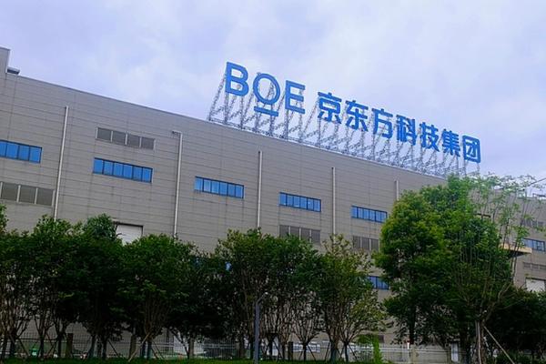
BOE's pivot to glass-based AI packaging could disrupt the supply chain for high-end AI chip manufacturing.
30-Second TL;DR
What Changed
BOE partnered with Corning to develop glass-based packaging substrates.
Why It Matters
BOE's entry into the AI supply chain signals a strategic diversification away from the cyclical display market into high-growth semiconductor packaging.
What To Do Next
Evaluate TGV-based packaging solutions for your hardware roadmap if you are building high-performance AI accelerator systems.
Key Points
- •BOE partnered with Corning to develop glass-based packaging substrates.
- •Glass substrates offer better dielectric loss and stability than organic alternatives for AI chips.
- •BOE has completed full-process automation and is currently sending samples to clients.
- •Mass commercialization is expected in 2-3 years.
Deep Insight
AI-generated analysis for this event — not the original article.
Enhanced Key Takeaways
- •BOE's move into glass substrates leverages its existing expertise in TFT-LCD and OLED glass processing, repurposing high-precision lithography and panel-level packaging equipment.
- •The transition to glass substrates is driven by the need to support higher interconnect density and larger package sizes required by HBM (High Bandwidth Memory) and multi-die chiplet architectures.
- •Glass substrates provide superior flatness and thermal expansion coefficient (CTE) matching with silicon, which significantly reduces warpage issues common in large-scale organic substrates during high-temperature reflow processes.
- •BOE is positioning this technology as a strategic component of its '1+4+N' strategy, aiming to diversify revenue streams beyond display panels into the semiconductor materials and equipment ecosystem.
- •The partnership with Corning involves utilizing specialized glass compositions that offer high mechanical strength and electrical insulation properties specifically engineered for high-frequency AI signal transmission.
Competitor Analysis
- BOE (Glass)
- Sampling
- Intel (Glass)
- Pilot/Development
- SKC/Absolics (Glass)
- Pilot/Development
- BOE (Glass)
- Display-to-Semiconductor Pivot
- Intel (Glass)
- Internal AI/Server CPUs
- SKC/Absolics (Glass)
- Dedicated Glass Substrate Foundry
- BOE (Glass)
- Existing Large-Panel Infrastructure
- Intel (Glass)
- Advanced Packaging Ecosystem
- SKC/Absolics (Glass)
- Material Science Specialization
| Feature | BOE (Glass) | Intel (Glass) | SKC/Absolics (Glass) |
|---|---|---|---|
| Status | Sampling | Pilot/Development | Pilot/Development |
| Primary Focus | Display-to-Semiconductor Pivot | Internal AI/Server CPUs | Dedicated Glass Substrate Foundry |
| Key Advantage | Existing Large-Panel Infrastructure | Advanced Packaging Ecosystem | Material Science Specialization |
Technical Deep Dive
- Glass substrates utilize Through-Glass Vias (TGV) to replace traditional Through-Silicon Vias (TSV) or organic substrate drilling, allowing for higher density interconnects.
- The material exhibits a lower dielectric constant (Dk) and dielectric loss (Df), which minimizes signal attenuation in high-speed data transmission environments.
- Enhanced thermal stability allows for higher power density chips, as glass can withstand higher operating temperatures without significant dimensional deformation.
- The manufacturing process integrates panel-level packaging (PLP) techniques, enabling the production of larger substrate sizes compared to traditional wafer-level processes, thereby improving cost-efficiency for large-die AI accelerators.
Future ImplicationsAI analysis grounded in cited sources
Timeline
- 2023-09BOE announces strategic shift to expand into semiconductor packaging and display-related material technologies.
- 2024-05BOE and Corning formalize collaboration on glass-based substrate development for advanced packaging.
- 2025-11BOE completes the installation of full-process automation lines for glass substrate production.
- 2026-04BOE begins shipping initial glass substrate samples to key AI chip design partners for validation.
Weekly AI Recap
Read this week's curated digest of top AI events →
AI-curated news aggregator. All content rights belong to original publishers.
Original source: 36氪 ↗
This is a summary, not the original. Read the source, or get the weekly briefing.
The weekly digest
One email a week. Unsubscribe anytime.