🇨🇳cnBeta (Full RSS)•較早收集於 5h
聯發科:記憶體是XPU瓶頸之一 佔50%成本
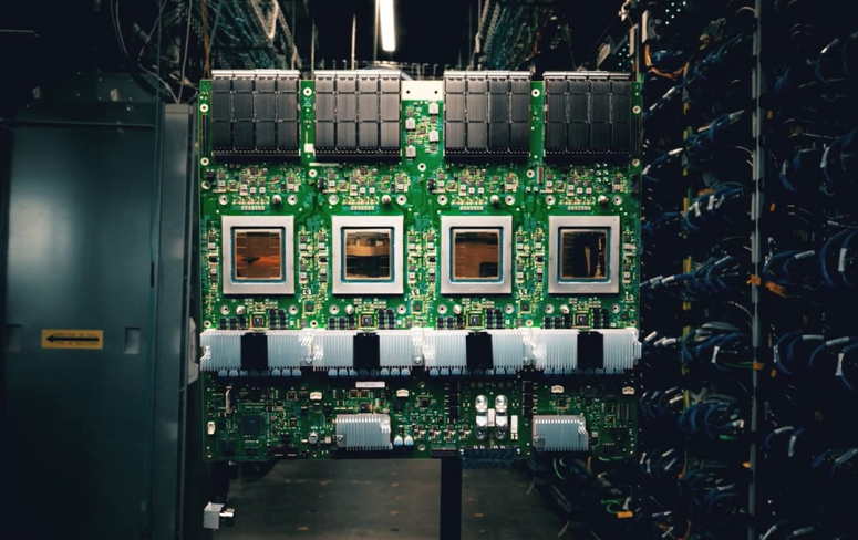
💡MediaTek: Memory hits 50% XPU costs – crucial for AI chip optimization
⚡ 30-Second TL;DR
有什麼變化
聯發科加入Google TPU v8項目
為什麼重要
強調AI加速器記憶體優化需求,引導硬體投資與可擴展AI運算設計。
下一步行動
Assess memory costs in your XPU prototypes using MediaTek's 50% benchmark.
誰應關注:Developers & AI Engineers
關鍵要點
- •聯發科加入Google TPU v8項目
- •記憶體是XPU主要瓶頸,佔50%成本
- •挑戰涵蓋運算、互聯、先進封裝
🧠 深度解析
背景與延伸:來自公開資料,非原文內容。引用 8 個來源。
🔑 增強重點摘要
- •MediaTek secured a $1 billion order from Google for TPU v7 chips manufactured on TSMC's 3nm process, with tape-out completed in September 2025 and mass production planned for Q4 2026[1].
- •Google is adopting a dual-sourcing strategy for TPUs, continuing with Broadcom for performance-oriented v7p variants while MediaTek handles inference-focused v7e, set for risk production by end of Q1 2026[3][4][7].
- •TSMC plans to increase CoWoS packaging capacity for MediaTek's Google TPU projects over sevenfold by 2027, from 20,000 wafers in 2026 to over 150,000 annually[3][4].
📊 競品分析▸ Show
| Feature | MediaTek (v7e/v8e) | Broadcom (v6p/v7p/v8) |
|---|---|---|
| Role | Inference-oriented TPUs, co-design | Performance/training TPUs, primary supplier[2][7][8] |
| Process Node | TSMC 3nm (v7e), 2nm planned (v8e) | TSMC advanced nodes (unspecified)[1][7] |
| CoWoS Wafers | 20K in 2026, >150K by 2027 | 200K pre-order in 2026 (+122% YoY)[4][7] |
| Timeline | Risk prod Q1 2026, mass Q4 2026 | Ongoing supply for current gens[3] |
🛠️ 技術深入
- •TPU v7 collaboration uses TSMC 3nm process for the chip, with MediaTek handling I/O modules for communication between main processors and peripherals[1][2].
- •TPU v8 planned on TSMC 2nm process, targeting 2028 launch, utilizing advanced CoWoS packaging technology[1].
- •v7e is inference-optimized variant, distinct from Broadcom's v7p training-focused version, supporting Google's diversification[7].
🔮 前景展望AI analysis grounded in cited sources
MediaTek's AI ASIC revenue to hit $1B in 2026
CEO Rick Tsai confirmed the first AI accelerator ASIC project is on track for $1 billion cloud ASIC revenue by 2026, driven by Google TPU orders[4].
TSMC CoWoS bottleneck to worsen with 7x capacity hike
Google reduces Nvidia reliance via MediaTek TPUs
Partnership diversifies TPU production from Broadcom, providing cost-effective alternatives to Nvidia GPUs for AI training and inference[2].
⏳ 時間線
2025-03
Reports emerge of Google-MediaTek TPU partnership for next-gen production[2]
2025-10
Google announces TPU v6 Trillium, setting stage for v7 diversification[2]
2025-09
MediaTek-Google TPU v7 tape-out completed on TSMC 3nm[1]
2025-12
MediaTek secures orders for TPU v7e and v8e, with TSMC CoWoS expansion plans[3][4]
2026-01
TPU v7e risk production begins by end of Q1[3][4]
2026-02
MediaTek CEO outlines XPU challenges including 50% memory cost bottleneck at Google TPU v8 project[ARTICLE]
📎 來源 (8)
Factual claims are grounded in the sources below. Forward-looking analysis is AI-generated interpretation.
- conevoelec.com — Post
- siliconangle.com — Google Reportedly Partnering Mediatek Next Generation Tpu Production
- technode.com — Mediatek Reportedly Secures Major Orders for Two Generations of Google Tpus
- trendforce.com — News Mediatek Reportedly Secures Google V7e V8e Tpu Orders Requests 7 Fold Cowos Increase From TSMC
- igorslab.de — Google Hunts Chips As Mediatek Becomes Secret Weapon in Tpu Race
- gist.github.com — 68c5afacfd3a3555ca834ba27415ba88
- eu.36kr.com — 3631956080985095
- counterpointresearch.com — AI Server Compute Asic Shipments to Triple by 2027
📰
AI 週報
閱讀本週精選 AI 大事摘要 →
👉相關動態
AI 策展新聞聚合。所有內容版權歸原始發布者所有。
原始來源: cnBeta (Full RSS) ↗
每週 AI 簡報
每週一封,可隨時退訂。