🇨🇳cnBeta (Full RSS)•Stalecollected in 5h
MediaTek: Memory 50% XPU Cost Bottleneck
💡MediaTek: Memory hits 50% XPU costs – crucial for AI chip optimization
⚡ 30-Second TL;DR
What Changed
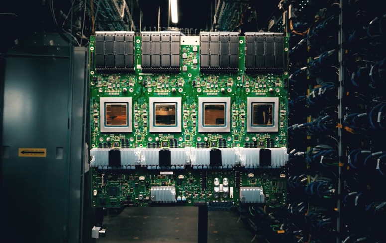
MediaTek joins Google TPU v8 project
Why It Matters
Emphasizes memory optimization needs for AI accelerators, guiding hardware investments and designs for scalable AI compute.
What To Do Next
Assess memory costs in your XPU prototypes using MediaTek's 50% benchmark.
Who should care:Developers & AI Engineers
🧠 Deep Insight
Web-grounded analysis with 8 cited sources.
🔑 Enhanced Key Takeaways
- •MediaTek secured a $1 billion order from Google for TPU v7 chips manufactured on TSMC's 3nm process, with tape-out completed in September 2025 and mass production planned for Q4 2026[1].
- •Google is adopting a dual-sourcing strategy for TPUs, continuing with Broadcom for performance-oriented v7p variants while MediaTek handles inference-focused v7e, set for risk production by end of Q1 2026[3][4][7].
- •TSMC plans to increase CoWoS packaging capacity for MediaTek's Google TPU projects over sevenfold by 2027, from 20,000 wafers in 2026 to over 150,000 annually[3][4].
📊 Competitor Analysis▸ Show
| Feature | MediaTek (v7e/v8e) | Broadcom (v6p/v7p/v8) |
|---|---|---|
| Role | Inference-oriented TPUs, co-design | Performance/training TPUs, primary supplier[2][7][8] |
| Process Node | TSMC 3nm (v7e), 2nm planned (v8e) | TSMC advanced nodes (unspecified)[1][7] |
| CoWoS Wafers | 20K in 2026, >150K by 2027 | 200K pre-order in 2026 (+122% YoY)[4][7] |
| Timeline | Risk prod Q1 2026, mass Q4 2026 | Ongoing supply for current gens[3] |
🛠️ Technical Deep Dive
- •TPU v7 collaboration uses TSMC 3nm process for the chip, with MediaTek handling I/O modules for communication between main processors and peripherals[1][2].
- •TPU v8 planned on TSMC 2nm process, targeting 2028 launch, utilizing advanced CoWoS packaging technology[1].
- •v7e is inference-optimized variant, distinct from Broadcom's v7p training-focused version, supporting Google's diversification[7].
🔮 Future ImplicationsAI analysis grounded in cited sources
MediaTek's AI ASIC revenue to hit $1B in 2026
CEO Rick Tsai confirmed the first AI accelerator ASIC project is on track for $1 billion cloud ASIC revenue by 2026, driven by Google TPU orders[4].
TSMC CoWoS bottleneck to worsen with 7x capacity hike
Google reduces Nvidia reliance via MediaTek TPUs
Partnership diversifies TPU production from Broadcom, providing cost-effective alternatives to Nvidia GPUs for AI training and inference[2].
⏳ Timeline
2025-03
Reports emerge of Google-MediaTek TPU partnership for next-gen production[2]
2025-10
Google announces TPU v6 Trillium, setting stage for v7 diversification[2]
2025-09
MediaTek-Google TPU v7 tape-out completed on TSMC 3nm[1]
2025-12
MediaTek secures orders for TPU v7e and v8e, with TSMC CoWoS expansion plans[3][4]
2026-01
TPU v7e risk production begins by end of Q1[3][4]
2026-02
MediaTek CEO outlines XPU challenges including 50% memory cost bottleneck at Google TPU v8 project[ARTICLE]
📎 Sources (8)
Factual claims are grounded in the sources below. Forward-looking analysis is AI-generated interpretation.
- conevoelec.com — Post
- siliconangle.com — Google Reportedly Partnering Mediatek Next Generation Tpu Production
- technode.com — Mediatek Reportedly Secures Major Orders for Two Generations of Google Tpus
- trendforce.com — News Mediatek Reportedly Secures Google V7e V8e Tpu Orders Requests 7 Fold Cowos Increase From TSMC
- igorslab.de — Google Hunts Chips As Mediatek Becomes Secret Weapon in Tpu Race
- gist.github.com — 68c5afacfd3a3555ca834ba27415ba88
- eu.36kr.com — 3631956080985095
- counterpointresearch.com — AI Server Compute Asic Shipments to Triple by 2027
📰
Weekly AI Recap
Read this week's curated digest of top AI events →
👉Related Updates


AI-curated news aggregator. All content rights belong to original publishers.
Original source: cnBeta (Full RSS) ↗