🇨🇳cnBeta (Full RSS)•最新收集於 10m
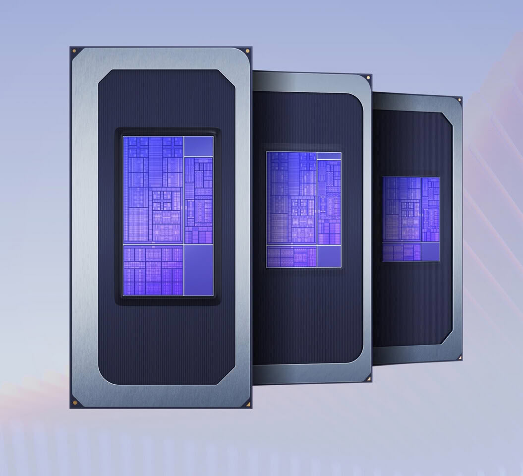
Intel 採用 ASML 新一代光刻機生產 Panther Lake 晶片
💡AI 硬體的關鍵基礎設施更新:Intel 的製造轉型將影響未來邊緣 AI 晶片的供應。
⚡ 30-Second TL;DR
有什麼變化
Intel 採用 ASML 最新光刻機製造旗艦晶片
為什麼重要
此合作透過利用卓越的製造精度,增強了 Intel 在高階行動晶片市場的競爭力。這標誌著 Intel 在重奪製程領先地位的代工策略中邁出了關鍵一步。
下一步行動
密切關注 Intel 的代工路線圖更新,以評估 AI 加速邊緣運算硬體的潛在產能變化。
誰應關注:Developers & AI Engineers
關鍵要點
- •Intel 採用 ASML 最新光刻機製造旗艦晶片
- •專注於 Panther Lake 架構的製造效率提升
- •策略性掌握先進半導體生產設備的使用
🧠 深度解析
AI-generated analysis for this event.
🔑 增強重點摘要
- •Intel 在 Panther Lake 的生產中導入了 ASML 的高數值孔徑(High-NA)EUV 光刻機,這是該技術在量產環境下的關鍵應用里程碑。
- •此製造流程結合了 Intel 18A 製程技術,旨在透過更精細的電路圖案化提升電晶體密度與能源效率。
- •Panther Lake 晶片採用了 Intel 的 Foveros 3D 封裝技術,將不同製程節點的晶片模組進行異質整合。
- •ASML 的 High-NA EUV 設備(EXE:5000 系列)具備 0.55 NA 光學系統,能有效降低多重曝光的需求,進而縮短生產週期並減少缺陷率。
- •Intel 透過與 ASML 的長期戰略合作,確保了該設備的優先供應權,藉此在與台積電(TSMC)的先進製程競爭中取得設備領先優勢。
📊 競品分析▸ Show
| 特性/競爭對手 | Intel Panther Lake | TSMC (Apple M-Series/N2) | Samsung Foundry (SF2) |
|---|---|---|---|
| 光刻技術 | High-NA EUV | EUV (0.33 NA) / Multi-patterning | EUV (0.33 NA) |
| 製程節點 | Intel 18A | N2 (2nm) | SF2 (2nm) |
| 封裝技術 | Foveros 3D | InFO / CoWoS | I-Cube |
| 市場定位 | 高效能筆電/AI PC | 高階行動運算/AI | 行動裝置/高效能運算 |
🛠️ 技術深入
- 採用 High-NA EUV 光刻技術,數值孔徑從 0.33 提升至 0.55,顯著提升解析度。
- 整合 Intel 18A 製程,引入 RibbonFET 全環繞閘極電晶體架構。
- 應用 PowerVia 背面供電技術,將供電網路移至晶圓背面,減少訊號干擾並提升電壓穩定性。
- 支援 Panther Lake 的模組化設計,包含運算晶片(Compute Tile)、繪圖晶片(Graphics Tile)與 I/O 晶片,透過 Foveros 進行堆疊。
🔮 前景展望AI analysis grounded in cited sources
Intel 將在 2026 年底前實現 18A 製程的全面成本優化。
隨著 High-NA EUV 設備的產能爬坡,單片晶圓的曝光成本預計將因減少多重曝光步驟而顯著下降。
Panther Lake 將成為 Intel 奪回筆電市場市佔率的核心產品。
該晶片在能效比上的顯著提升,使其在 AI PC 領域具備與 Apple Silicon 直接競爭的硬體基礎。
⏳ 時間線
2022-01
Intel 宣佈與 ASML 達成協議,成為全球首家接收 High-NA EUV 設備的客戶。
2023-12
ASML 向 Intel 交付首台 EXE:5000 High-NA EUV 光刻機。
2024-05
Intel 確認 18A 製程已進入風險試產階段,並將應用於 Panther Lake。
2025-09
Intel 成功利用 High-NA EUV 設備完成 Panther Lake 的晶圓試產驗證。
2026-06
Intel 正式啟動 Panther Lake 的大規模量產流程。
📰
AI 週報
閱讀本週精選 AI 大事摘要 →
👉相關動態


AI 策展新聞聚合。所有內容版權歸原始發布者所有。
原始來源: cnBeta (Full RSS) ↗