🌍The Next Web (TNW)•Freshcollected in 49m
ASML’s $400M machine prints first laptop processors

💡See how the world's most expensive chip machines are accelerating the next generation of AI-capable processors.
⚡ 30-Second TL;DR
What Changed
High NA EUV machines cost approximately $400 million each.
Why It Matters
The early adoption of High NA EUV accelerates the roadmap for high-performance AI chips. This allows for denser, more efficient transistors, directly benefiting future AI compute hardware.
What To Do Next
Monitor Intel's Panther Lake performance benchmarks to gauge the real-world efficiency gains of High NA EUV manufacturing.
Who should care:Developers & AI Engineers
Key Points
- •High NA EUV machines cost approximately $400 million each.
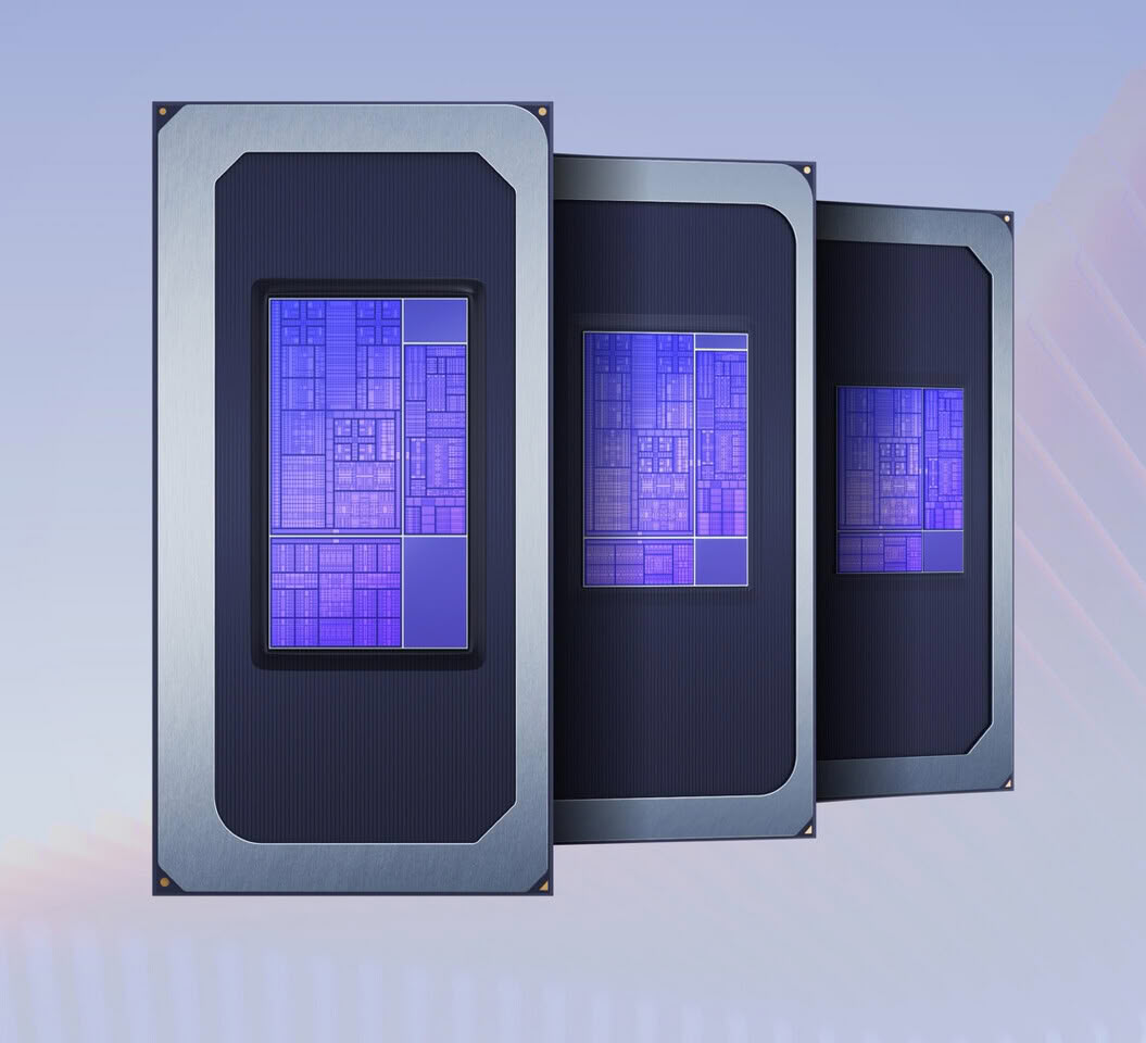
- •The technology is being used for Intel's Panther Lake processor layers.
- •This deployment is ahead of the previously expected 14A node timeline.
🧠 Deep Insight
AI-generated analysis for this event.
🔑 Enhanced Key Takeaways
- •The High NA EUV system utilized is the ASML EXE:5000, which features a numerical aperture of 0.55 compared to the 0.33 NA of previous-generation EUV machines.
- •Intel's adoption of High NA EUV is critical for its '14A' process node, which aims to extend Moore's Law by enabling higher transistor density and reduced power consumption.
- •The transition to High NA EUV requires a shift to anamorphic lenses, which magnify differently in the X and Y axes to maintain resolution across the entire exposure field.
- •ASML's High NA machines require significantly more power and a larger cleanroom footprint than standard EUV systems, necessitating specialized facility upgrades at Intel's Fab D1X in Oregon.
- •The deployment of this technology is part of Intel's '5 nodes in 4 years' strategy, intended to regain process leadership from TSMC.
📊 Competitor Analysis▸ Show
| Feature | ASML High NA EUV (EXE:5000) | TSMC/Canon/Nikon Alternatives |
|---|---|---|
| Numerical Aperture | 0.55 NA | 0.33 NA (Standard EUV) / Nanoimprint (Canon) |
| Primary Use Case | Leading-edge logic (14A/10A) | High-volume manufacturing (N3/N2) |
| Pricing | ~$400M per unit | N/A (TSMC utilizes existing EUV fleet) |
| Benchmarks | Highest resolution/density | Higher throughput/lower cost per wafer |
🛠️ Technical Deep Dive
- Numerical Aperture: Increased from 0.33 to 0.55, allowing for a resolution improvement of approximately 1.7x.
- Anamorphic Optics: Uses a catoptric system with a 4x magnification in one axis and 8x in the other to overcome the physical size limitations of the reticle.
- Throughput: Designed to process over 200 wafers per hour, maintaining productivity levels despite the increased complexity of the optical path.
- Resolution: Capable of printing features down to 8nm, significantly reducing the need for multi-patterning steps required by lower NA systems.
🔮 Future ImplicationsAI analysis grounded in cited sources
High NA EUV will become the industry standard for sub-2nm logic production by 2028.
The resolution limits of 0.33 NA EUV necessitate the adoption of 0.55 NA technology to avoid the yield-killing complexity of multi-patterning at smaller nodes.
Intel will achieve cost parity with TSMC for advanced nodes within three years.
By reducing the number of lithography steps through higher resolution, Intel can offset the massive capital expenditure of the $400M machines.
⏳ Timeline
2018-12
Intel places the first order for ASML's High NA EUV pilot equipment.
2023-12
ASML ships the first EXE:5000 High NA EUV system to Intel's Oregon facility.
2024-04
Intel successfully achieves first light on the High NA EUV machine.
2026-07
Intel begins printing layers for Panther Lake processors using High NA EUV.
📰
Weekly AI Recap
Read this week's curated digest of top AI events →
👉Related Updates


AI-curated news aggregator. All content rights belong to original publishers.
Original source: The Next Web (TNW) ↗