YMTC's IPO Signals a NAND Comeback
💡YMTC's IPO could reshape China's AI-memory supply chain after export controls stalled its NAND expansion.
⚡ 30-Second TL;DR
What Changed
YMTC officially started its IPO process on May 19, passed sponsorship review on August 19, and was accepted on August 21.
Why It Matters
A successful IPO could provide YMTC with the capital needed to close the gap in NAND process scale and cost, strengthening China's domestic memory supply for AI servers and other data-intensive systems. However, equipment restrictions and intense competition from Samsung, SK hynix, and Micron remain major execution risks.
What To Do Next
For AI hardware planning, benchmark YMTC NAND availability, endurance, and read/write latency against Samsung, SK hynix, and Micron before committing to a storage design.
Key Points
- •YMTC officially started its IPO process on May 19, passed sponsorship review on August 19, and was accepted on August 21.
- •The company plans to raise RMB 33 billion for production-line upgrades and next-generation architecture research.
- •Its Xtacking architecture separates NAND arrays from peripheral circuits and connects them through wafer-level hybrid bonding.
- •YMTC's mass-produced products have advanced to 267 layers, while the industry is moving toward 300- to 400-layer NAND.
- •U.S. export controls on equipment for 128-layer-and-above NAND disrupted YMTC's scaling and supply-chain development.
🧠 Deep Insight
Background and context from public sources — not the original article. 12 sources cited.
🔑 Enhanced Key Takeaways
- •YMTC's IPO is the largest in the history of the Shanghai STAR Market, exceeding the initial fundraising targets of both SMIC and CXMT.
- •The company achieved a massive financial turnaround in Q1 2026, reporting a net profit of RMB 33.38 billion on revenues of RMB 47.04 billion.
- •YMTC's NAND Flash gross margin expanded significantly to 78.73% in Q1 2026, up from approximately 35% in the previous year.
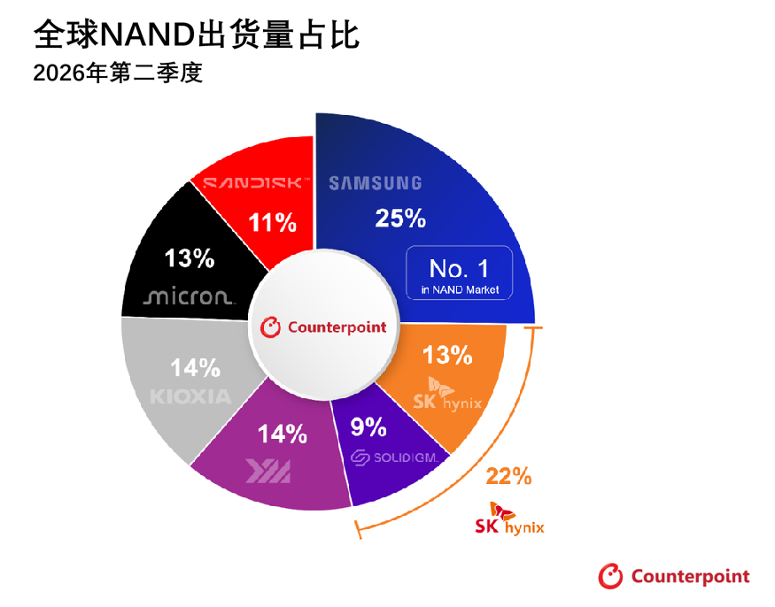
- •As of Q2 2026, YMTC has secured a 14% global NAND market share, positioning it as the third-largest supplier worldwide behind Samsung and SK Hynix.
- •The company's current production utilizes the Xtacking 4.0 architecture, which is central to its ability to maintain competitiveness despite ongoing U.S. Entity List restrictions.
📊 Competitor Analysis▸ Show
| Feature | YMTC | Samsung | SK Hynix |
|---|---|---|---|
| Market Share (Q2 2026) | 14% | Leader | Top 2 |
| Primary Focus | Consumer NAND | Enterprise/Data Center | Enterprise/Data Center |
| Architecture | Xtacking 4.0 | V-NAND | 4D NAND |
🛠️ Technical Deep Dive
- Xtacking 4.0 Architecture: Utilizes advanced wafer-level hybrid bonding to decouple the CMOS peripheral circuit from the NAND array, allowing for independent optimization of both components.
- Layer Density: Current mass production is at 267 layers, with active R&D focused on scaling beyond 300 layers.
- Manufacturing Focus: Proceeds are specifically allocated to yield improvement and capacity expansion for high-layer-count 3D NAND production lines.
🔮 Future ImplicationsAI analysis grounded in cited sources
⏳ Timeline
📎 Sources (12)
Factual claims are grounded in the sources below. Forward-looking analysis is AI-generated interpretation.
Weekly AI Recap
Read this week's curated digest of top AI events →
👉Related Updates
AI-curated news aggregator. All content rights belong to original publishers.
Original source: 虎嗅 ↗
This is a summary, not the original. Read the source, or get the weekly briefing.
Weekly AI briefing
One email a week. Unsubscribe anytime.