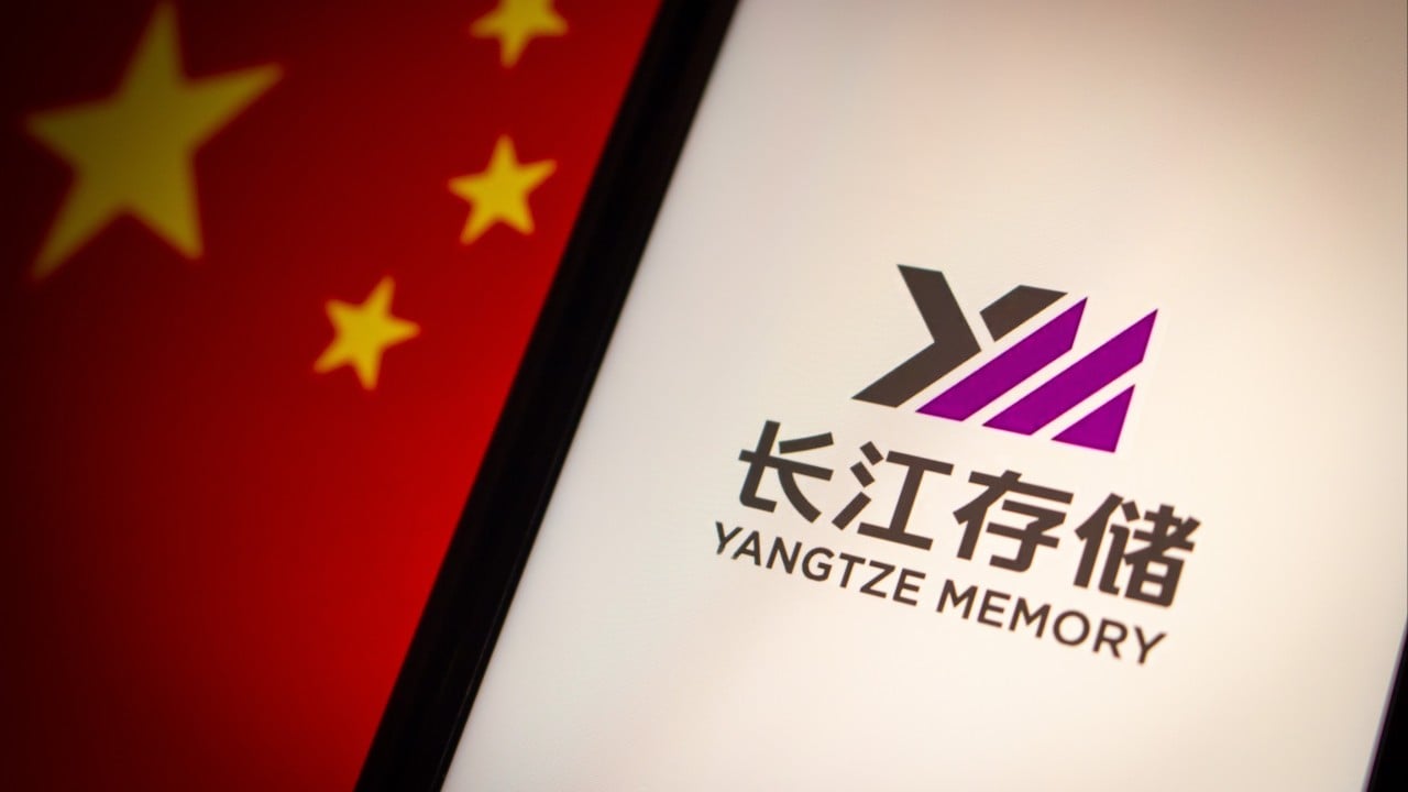
YMTC Enters Global NAND Top Three
💡YMTC’s rise could reshape the SSD supply base behind AI data centres.
⚡ 30-Second TL;DR
What Changed
YMTC accounted for 14% of global NAND bit shipments in the second quarter.
Why It Matters
Stronger YMTC supply could increase competition in enterprise SSD and data-centre storage markets. For AI infrastructure operators, broader NAND supplier diversity may improve sourcing resilience, although performance, qualification, and geopolitical risks still require evaluation.
What To Do Next
Use fio to benchmark YMTC-based SSD samples against your current storage fleet for AI dataset reads, checkpoint writes, endurance, and latency before changing suppliers.
Key Points
- •YMTC accounted for 14% of global NAND bit shipments in the second quarter.
- •The company narrowly overtook Japan-based Kioxia to reach third place by shipment volume.
- •Its progress could help China reduce the gap with global leaders in high-value data-centre storage.
🧠 Deep Insight
AI-generated analysis for this event.
🔑 Enhanced Key Takeaways
- •YMTC's rapid growth has been driven by its proprietary Xtacking architecture, which separates the manufacturing of peripheral circuits and memory cell arrays to improve density and yield.
- •The company has faced significant headwinds from US export controls, specifically the 2022 inclusion on the Entity List, which restricted its access to advanced semiconductor manufacturing equipment.
- •Despite trade restrictions, YMTC has successfully pivoted to domestic supply chains and increased its reliance on Chinese-made lithography and etching tools to sustain production.
- •Market analysts note that YMTC's aggressive pricing strategy in the consumer SSD market has been a primary lever for gaining market share, putting pressure on margins for incumbents like Samsung and SK Hynix.
- •The shift to 232-layer and higher 3D NAND nodes has been critical for YMTC to achieve the bit shipment volumes necessary to compete in the enterprise and data-center segments.
📊 Competitor Analysis▸ Show
| Feature | YMTC | Samsung | Kioxia | Micron |
|---|---|---|---|---|
| Primary Tech | Xtacking 3D NAND | V-NAND | BiCS FLASH | Replacement Gate |
| Market Focus | Value/Consumer/Domestic | Enterprise/Mobile/High-End | Enterprise/Client | Enterprise/Cloud/AI |
| Supply Chain | High Domestic Integration | Global/Diversified | Global/Japan-centric | Global/US-centric |
🛠️ Technical Deep Dive
- Xtacking Architecture: Utilizes a wafer-to-wafer bonding process that allows peripheral circuits and NAND memory cells to be processed on separate wafers before being bonded together.
- Layer Count: YMTC has successfully transitioned to mass production of 232-layer 3D NAND, enabling higher bit density per square millimeter.
- Interface Speed: Current generation products support high-speed interfaces (up to 2400 MT/s) to meet the bandwidth requirements of modern PCIe Gen 5 SSDs.
- Die Size Efficiency: The modular nature of the Xtacking design allows for smaller die sizes compared to traditional monolithic 3D NAND structures, improving wafer utilization.
🔮 Future ImplicationsAI analysis grounded in cited sources
⏳ Timeline
Weekly AI Recap
Read this week's curated digest of top AI events →
👉Related Updates

AI-curated news aggregator. All content rights belong to original publishers.
Original source: SCMP Technology ↗