Xunlin Raises Nearly ¥200M for Glass Substrates
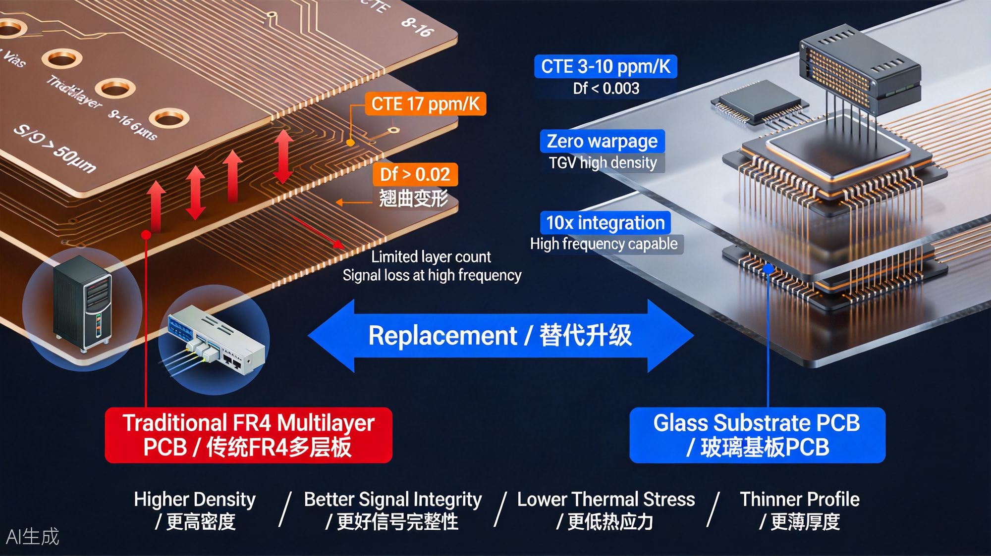
Glass substrates may become a practical answer to AI server PCB shortages and rising organic-substrate costs.
30-Second TL;DR
What Changed
New investors include Inno Fund, Qiancheng Capital, Haycm, and Lianfang, while existing shareholders continued investing.
Why It Matters
The financing signals growing investor confidence that glass substrates can address AI server PCB and advanced-packaging constraints. If Xunlin achieves competitive cost and yield at scale, its technology could reduce dependence on expensive organic substrates and overseas ABF suppliers.
What To Do Next
Map your AI server or advanced-packaging bill of materials against glass PCB and glass-core substrate availability, then identify qualification tests needed for a supplier pilot.
Key Points
- •New investors include Inno Fund, Qiancheng Capital, Haycm, and Lianfang, while existing shareholders continued investing.
- •The company plans to expand glass-substrate capacity, build packaging lines, improve process precision, and develop optical communications applications.
- •Xunlin operates a 300,000-square-meter annual-capacity full-process factory covering cutting, thinning, TGV drilling, PVD metallization, electroplating, patterning, and solder mask.
- •Its glass-substrate PCB products for Mini LED backlighting, COB direct displays, and MIP display modules have entered mass shipment.
- •The company is targeting PCB replacement first, followed by ABF substrate replacement from 2027 and interposer applications through 2027-2030.
Deep Insight
AI-generated analysis for this event — not the original article.
Enhanced Key Takeaways
- •Xunlin Technology (also known as Xunlin Microelectronics) is strategically positioning itself to capitalize on the industry-wide shift toward glass substrates as a solution to the physical limitations of organic ABF substrates in high-performance computing.
- •The company's TGV (Through Glass Via) technology is a critical differentiator, enabling higher density interconnects and better thermal stability compared to traditional silicon or organic-based interposers.
- •Xunlin's facility in China represents one of the few vertically integrated manufacturing sites capable of handling the full glass substrate process chain, reducing reliance on external supply chains for specialized metallization and patterning.
- •The company has actively engaged in collaborative R&D with downstream display manufacturers to optimize the coefficient of thermal expansion (CTE) matching between glass substrates and Mini LED/MIP components.
- •The rapid succession of three financing rounds in six months indicates strong institutional confidence in Xunlin's ability to scale production ahead of the projected 2027 industry inflection point for glass substrate adoption in advanced packaging.
Competitor Analysis
- Xunlin Technology
- Mini LED/MIP & PCB Replacement
- Absolics (SKC)
- High-Performance Computing (HPC)
- Intel (Glass Substrate Division)
- Data Center/AI Packaging
- Corning
- Glass Material Science/Supply
- Xunlin Technology
- Mass Production (Display)
- Absolics (SKC)
- Pilot/Early Production
- Intel (Glass Substrate Division)
- R&D/Advanced Pilot
- Corning
- Material/Substrate Supply
- Xunlin Technology
- Mass Shipment (Display)
- Absolics (SKC)
- Pre-Commercial
- Intel (Glass Substrate Division)
- Development/Validation
- Corning
- Supplier
| Feature | Xunlin Technology | Absolics (SKC) | Intel (Glass Substrate Division) | Corning |
|---|---|---|---|---|
| Primary Focus | Mini LED/MIP & PCB Replacement | High-Performance Computing (HPC) | Data Center/AI Packaging | Glass Material Science/Supply |
| TGV Capability | Mass Production (Display) | Pilot/Early Production | R&D/Advanced Pilot | Material/Substrate Supply |
| Market Stage | Mass Shipment (Display) | Pre-Commercial | Development/Validation | Supplier |
Technical Deep Dive
- TGV (Through Glass Via) Drilling: Utilizes high-precision laser ablation to create vertical interconnects with aspect ratios optimized for signal integrity.
- PVD Metallization: Employs physical vapor deposition to ensure uniform seed layer adhesion on glass surfaces, which are notoriously difficult to metallize compared to organic substrates.
- Patterning Precision: Achieves fine-pitch lithography capable of supporting the high-density requirements of next-generation interposers.
- CTE Matching: Engineered glass compositions designed to match the thermal expansion characteristics of silicon chips, reducing warpage and mechanical stress during thermal cycling.
- Surface Treatment: Proprietary chemical etching processes used to enhance glass surface roughness for improved copper adhesion without compromising dielectric properties.
Future ImplicationsAI analysis grounded in cited sources
Timeline
- 2026-02Xunlin completes initial financing round to accelerate TGV process development.
- 2026-05Company achieves mass shipment milestone for Mini LED and MIP glass-substrate modules.
- 2026-08Xunlin closes nearly 200 million yuan Series B round to expand capacity and R&D.
Weekly AI Recap
Read this week's curated digest of top AI events →
AI-curated news aggregator. All content rights belong to original publishers.
Original source: 36氪 ↗
This is a summary, not the original. Read the source, or get the weekly briefing.
The weekly digest
One email a week. Unsubscribe anytime.