🇨🇳cnBeta (Full RSS)•Freshcollected in 8m
Soviet Chip Push: Spies, Reverse Eng, Ultimate Failure
💡Soviet chip flops show why ecosystem > hardware for AI semis
⚡ 30-Second TL;DR
What Changed
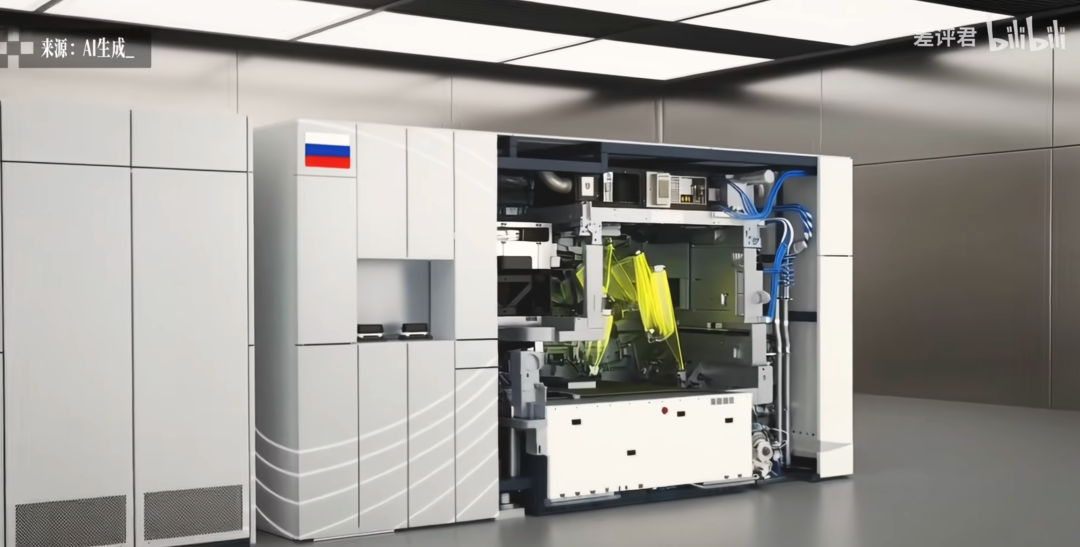
350nm lithography machine added to Russia's national system
Why It Matters
Reveals ecosystem gaps in chip tech beyond hardware, informing current AI semiconductor geopolitics and self-reliance strategies.
What To Do Next
Study Planar’s legacy docs for insights on scaling lithography in AI chip prototyping.
Who should care:Researchers & Academics
🧠 Deep Insight
AI-generated analysis for this event.
🔑 Enhanced Key Takeaways
- •The 350nm lithography machine is part of a broader Russian state-funded initiative, 'Project Lithography,' aimed at achieving technological sovereignty following severe Western sanctions that cut off access to advanced EUV and DUV equipment.
- •Planar, a Belarusian state-owned enterprise, has historically specialized in photolithography equipment for the Soviet military-industrial complex, and this collaboration represents a revival of specialized optics and precision engineering capabilities that had largely atrophied since the 1990s.
- •Industry analysts note that while 90nm production is sufficient for certain legacy military and industrial control systems, it remains significantly behind the global state-of-the-art, which has moved toward 2nm and 3nm nodes, limiting the machine's utility for modern consumer electronics or high-performance computing.
🛠️ Technical Deep Dive
- The machine utilizes a g-line (436 nm) or i-line (365 nm) mercury lamp light source, which is standard for older lithography systems but lacks the resolution required for sub-90nm features.
- The 350nm designation refers to the resolution limit of the optical system, while the 90nm capability is achieved through advanced process integration and multi-patterning techniques.
- The system relies on traditional refractive optics rather than the reflective EUV (Extreme Ultraviolet) optics used in modern ASML machines, making it significantly larger and less efficient in terms of throughput.
🔮 Future ImplicationsAI analysis grounded in cited sources
Russia will fail to achieve commercial-scale semiconductor independence by 2030.
The reliance on legacy 90nm technology creates a massive performance and power-efficiency gap that cannot be bridged without access to modern global supply chains and advanced materials.
The ZNTC-Planar machine will be restricted exclusively to military and critical infrastructure applications.
The high cost per wafer and low throughput of legacy-based lithography make it economically unviable for competitive consumer electronics production.
⏳ Timeline
2022-03
Western sanctions lead to a total ban on the export of advanced semiconductor manufacturing equipment to Russia.
2023-05
Russian Ministry of Industry and Trade announces the 'Project Lithography' initiative to develop domestic manufacturing tools.
2024-11
ZNTC and Planar announce the successful testing of a prototype lithography system capable of 350nm resolution.
2026-04
Official integration of the 350nm lithography machine into the Russian national industrial production framework.
📰
Weekly AI Recap
Read this week's curated digest of top AI events →
👉Related Updates


AI-curated news aggregator. All content rights belong to original publishers.
Original source: cnBeta (Full RSS) ↗