💰钛媒体•Freshcollected in 2h
TSMC Unveils EUV-Bypassing Node
💡TSMC's EUV bypass unlocks cheaper AI chip nodes faster
⚡ 30-Second TL;DR
What Changed
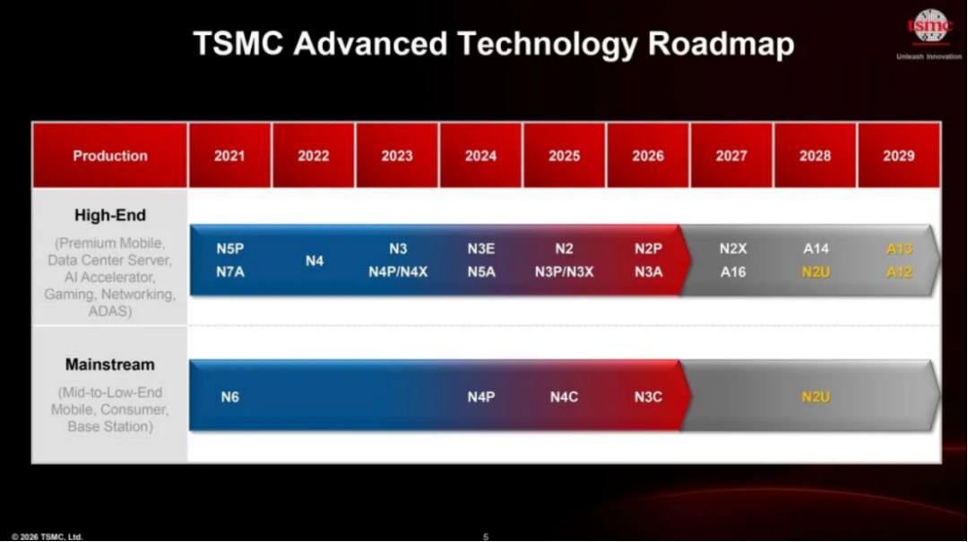
TSMC's killer process node bypasses top EUV
Why It Matters
Reduces reliance on ASML's priciest EUV tools, potentially lowering AI chip costs. Accelerates TSMC's node roadmap for Nvidia GPUs and AI accelerators. Signals shift in semiconductor supply chain dynamics.
What To Do Next
Assess TSMC A16 node specs for your next AI ASIC tape-out planning.
Who should care:Enterprise & Security Teams
🧠 Deep Insight
AI-generated analysis for this event.
🔑 Enhanced Key Takeaways
- •The node, internally referred to as 'N-Zero' or similar non-EUV-dependent advanced process, utilizes multi-patterning techniques with DUV (Deep Ultraviolet) lithography to achieve density targets previously thought to require High-NA EUV.
- •This strategic shift is primarily driven by the escalating costs and supply chain constraints associated with ASML's High-NA EUV systems, allowing TSMC to maintain margins on mid-to-high-end chip production.
- •Industry analysts suggest this node is specifically optimized for AI inference accelerators and mobile SoCs where power efficiency is prioritized over the absolute transistor density gains offered by the latest EUV generations.
📊 Competitor Analysis▸ Show
| Feature | TSMC 'N-Zero' (Non-EUV) | Intel 18A (High-NA EUV) | Samsung 2nm (GAA/EUV) |
|---|---|---|---|
| Lithography | DUV Multi-patterning | High-NA EUV | EUV |
| Cost Structure | Lower (Lower CapEx) | Higher (High CapEx) | Moderate |
| Target Segment | AI Inference/Mobile | HPC/Data Center | Mobile/Foundry |
🛠️ Technical Deep Dive
- •Utilizes advanced self-aligned quadruple patterning (SAQP) to overcome DUV resolution limits.
- •Integrates proprietary material science breakthroughs in photoresist chemistry to improve pattern fidelity without EUV light sources.
- •Employs a modified FinFET architecture optimized for lower voltage operation to compensate for the increased interconnect complexity inherent in multi-patterning designs.
- •Reduces reliance on stochastic-prone EUV processes, potentially improving yield rates for specific logic-heavy chip designs.
🔮 Future ImplicationsAI analysis grounded in cited sources
TSMC will reduce its dependency on ASML's High-NA EUV roadmap by at least 20% over the next three years.
The successful deployment of a high-performance DUV-based node provides a viable, lower-cost alternative for a significant portion of TSMC's product portfolio.
Foundry pricing for mid-tier AI chips will stabilize despite rising lithography equipment costs.
By bypassing the most expensive EUV tools, TSMC can decouple its pricing strategy from the inflationary pressures of next-generation lithography hardware.
⏳ Timeline
2023-10
TSMC signals intent to extend DUV capabilities for advanced nodes during investor briefing.
2024-06
Initial R&D reports emerge regarding 'EUV-bypass' patterning techniques.
2025-11
TSMC completes pilot production run of the new node with yield rates exceeding internal targets.
2026-05
Official unveiling of the EUV-bypassing node to the public.
📰
Weekly AI Recap
Read this week's curated digest of top AI events →
👉Related Updates


AI-curated news aggregator. All content rights belong to original publishers.
Original source: 钛媒体 ↗