🇨🇳cnBeta (Full RSS)•Freshcollected in 9m
SK Hynix 1c DRAM Yield at 80%, 190K Wafers EOY
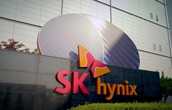
💡SK Hynix 1c DRAM ramp boosts HBM4E for next-gen AI GPUs (80% yield).
⚡ 30-Second TL;DR
What Changed
1c DRAM yield reached 80%
Why It Matters
Advances HBM supply chain for AI GPUs, easing bottlenecks for NVIDIA Blackwell and future training clusters.
What To Do Next
Request SK Hynix HBM4E samples to benchmark against HBM3E for AI inference setups.
Who should care:Enterprise & Security Teams
🧠 Deep Insight
AI-generated analysis for this event.
🔑 Enhanced Key Takeaways
- •The 1c node represents the sixth generation of 10nm-class DRAM, utilizing advanced EUV lithography to overcome scaling limitations inherent in previous 1b processes.
- •SK Hynix is prioritizing the 1c node specifically to address the thermal and power efficiency requirements of next-generation HBM4E stacks, which require higher density per die.
- •The aggressive capacity expansion to 190,000 wafers per month is supported by the conversion of legacy D1a/D1b lines to EUV-capable infrastructure, rather than solely relying on new fab construction.
📊 Competitor Analysis▸ Show
| Feature | SK Hynix (1c DRAM) | Samsung (1c DRAM) | Micron (1γ DRAM) |
|---|---|---|---|
| EUV Usage | High (Tripled investment) | High (Multi-layer) | Low (Selective usage) |
| HBM4E Readiness | Sampling 2026 | Sampling 2026 | Development phase |
| Yield Maturity | 80% (Reported) | Competitive (Internal) | Emerging |
🛠️ Technical Deep Dive
- Node: 1c (Sixth-gen 10nm-class).
- Lithography: Multi-patterning EUV (Extreme Ultraviolet) to reduce mask count and improve overlay accuracy.
- Architecture: High-aspect-ratio capacitor structures optimized for HBM4E vertical stacking.
- Power Management: Integrated logic-die improvements to support the higher bandwidth-per-watt requirements of HBM4E.
🔮 Future ImplicationsAI analysis grounded in cited sources
SK Hynix will maintain a dominant market share in the HBM4E segment through 2027.
Early yield maturity at the 1c node provides a significant cost-per-bit advantage over competitors still refining their EUV processes.
The 1c node will become the primary volume driver for SK Hynix's server DRAM revenue by Q4 2026.
The rapid ramp-up to 190,000 wafers per month indicates a strategic shift to replace lower-margin legacy nodes with high-density 1c production.
⏳ Timeline
2023-05
SK Hynix begins mass production of 1a nm DRAM.
2024-01
SK Hynix announces development of 1b nm DRAM with EUV technology.
2025-03
SK Hynix confirms successful pilot production of 1c DRAM.
2026-02
SK Hynix reports 80% yield milestone for 1c DRAM node.
📰
Weekly AI Recap
Read this week's curated digest of top AI events →
👉Related Updates

AI-curated news aggregator. All content rights belong to original publishers.
Original source: cnBeta (Full RSS) ↗