SK Hynix Unveils HBM4E 48GB 12-Layer Memory
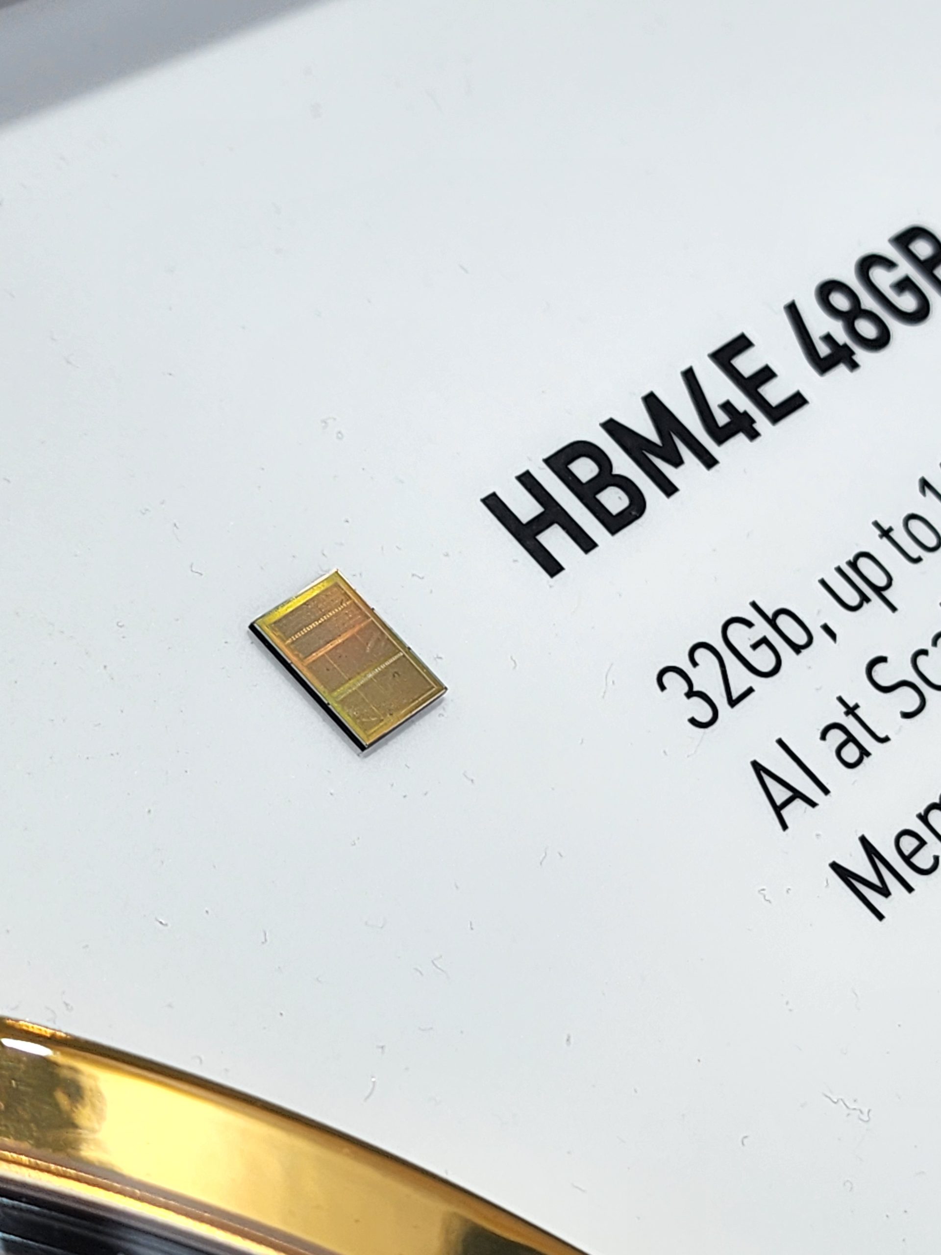
💡4TB/s bandwidth: See how the next generation of HBM memory will accelerate your large-scale AI model inference.
⚡ 30-Second TL;DR
What Changed
48GB capacity with 12-layer stacking architecture
Why It Matters
This advancement significantly alleviates the memory bottleneck for large-scale generative AI and inference models. It enables faster training and deployment of massive parameter models.
What To Do Next
Monitor the availability of HBM4E-compatible hardware for your upcoming cluster upgrades to maximize inference throughput.
Key Points
- •48GB capacity with 12-layer stacking architecture
- •Single-chip bandwidth reaches 4TB/s
- •Optimized for next-gen AI data center GPU platforms from Nvidia and AMD
🧠 Deep Insight
Background and context from public sources — not the original article. 16 sources cited.
🔑 Enhanced Key Takeaways
- •Samsung Electronics shipped the industry's first 12-layer HBM4E samples to major global customers on May 29, 2026, claiming a lead of at least several months over rival SK Hynix in the race to supply next-generation AI accelerators.
- •The official HBM4 specification, released by JEDEC in April 2025, introduced a fundamental architectural overhaul by doubling the interface width to 2048 bits and enabling the logic base layer to be manufactured using advanced foundry logic nodes (e.g., 4nm or 5nm), which allows for the integration of custom controllers or basic compute functions directly into the memory stack.
- •Micron Technology plans to begin mass production of HBM4E in 2027, intending to use its 10nm-class sixth-generation 1-gamma (1γ) process for the core dies and shifting to TSMC for the base die, a change from its internal base die production for HBM4.
- •Samsung's HBM4E samples deliver a stable pin speed of 14 gigabits-per-second (Gbps), scalable up to 16 Gbps, and provide a single-stack bandwidth of 3.6 terabytes per second (TB/s), alongside improvements in energy efficiency and thermal resistance compared to HBM4.
- •The unprecedented demand for HBM from the AI sector has led to compounded price increases for DRAM and HBM, some exceeding 200% since early 2025, with HBM production crowding out commodity DRAM capacity.
📊 Competitor Analysis▸ Show
| Feature/Company | SK Hynix (HBM4E) | Samsung (HBM4E Samples) | Micron (HBM4E Plans) |
|---|---|---|---|
| Capacity (per stack) | 48GB (12-layer) | 48GB (12-layer), with plans for 32GB (8-layer) and 64GB (16-layer) | Mass production in 2027, with 1γ process for core dies |
| Bandwidth (per stack) | 4TB/s | 3.6 TB/s (stable 14 Gbps, scalable to 16 Gbps pin speed) | Not specified for HBM4E, HBM4 offers >2.8 TB/s |
| Base Die Manufacturing | TSMC (reportedly 3nm process) | Samsung Foundry (4nm process) | TSMC (for HBM4E) |
| Core Die Manufacturing | Not specified for HBM4E | 6th-gen 10nm-class DRAM process (1c) | 10nm-class 6th-gen 1-gamma (1γ) process |
| Sample Availability | Showcased at Computex 2026 (June 2026) | Shipped May 29, 2026 | Mass production in 2027 |
🛠️ Technical Deep Dive
- The HBM4 standard, finalized in April 2025, features a 2048-bit interface with 32 independent channels and 64 pseudo-channels, doubling the interface width of HBM3E.
- HBM4's core voltage is reduced to 1.05V from 1.1V in HBM3/3E, contributing to improved power efficiency.
- The standard incorporates Directed Refresh Management (DRFM) to enhance reliability, particularly for higher stack heights.
- A significant architectural change in HBM4 is the transition of the logic base layer to advanced foundry logic nodes (e.g., 4nm or 5nm), allowing for the integration of custom controllers or basic compute functions directly into the memory stack.
- Samsung's HBM4E samples utilize its 6th-generation 10nm-class DRAM process ('1c') for memory dies and its in-house 4nm foundry process for the logic base die.
- Samsung's HBM4E offers a 16% improvement in energy efficiency and over 14% enhancement in thermal resistance compared to HBM4.
- HBM4 architecture is projected to reduce total system power consumption by 20-30% and triple training speed for AI models exceeding 2 trillion parameters.
🔮 Future ImplicationsAI analysis grounded in cited sources
⏳ Timeline
📎 Sources (16)
Factual claims are grounded in the sources below. Forward-looking analysis is AI-generated interpretation.
Weekly AI Recap
Read this week's curated digest of top AI events →
👉Related Updates
AI-curated news aggregator. All content rights belong to original publishers.
Original source: cnBeta (Full RSS) ↗
This is a summary, not the original. Read the source, or get the weekly briefing.
The weekly digest
One email a week. Unsubscribe anytime.