SK hynix Starts $4B U.S. HBM Plant
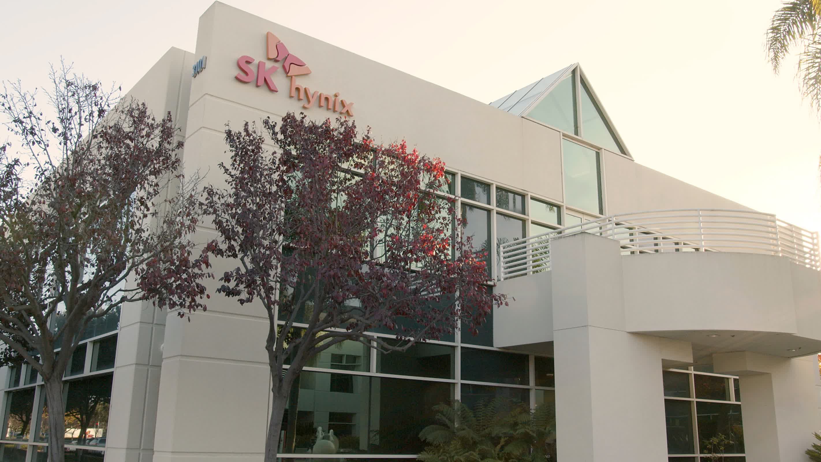
💡AI demand depends on HBM—SK hynix just started building a major U.S. packaging hub.
⚡ 30-Second TL;DR
What Changed
The facility is being built on a 133.5-acre site in West Lafayette, Indiana.
Why It Matters
A U.S.-based HBM packaging site could improve supply-chain resilience for AI accelerators and data-center operators. It may also increase domestic access to advanced memory packaging as demand for AI computing continues to grow.
What To Do Next
Review your AI accelerator procurement plans and ask suppliers whether future HBM capacity will come from SK hynix’s U.S. packaging operation.
Key Points
- •The facility is being built on a 133.5-acre site in West Lafayette, Indiana.
- •Investment in the plant exceeds $4 billion.
- •It will be SK hynix’s first U.S. facility dedicated to HBM packaging.
- •The project supports efforts to rebuild strategic semiconductor supply chains in the United States.
🧠 Deep Insight
Background and context from public sources — not the original article. 17 sources cited.
🔑 Enhanced Key Takeaways
- •The facility is designated to specialize in advanced back-end packaging and testing, specifically focusing on vertical chip stacking rather than front-end wafer fabrication.
- •The project is supported by the U.S. CHIPS and Science Act, securing up to $458 million in direct funding and an additional $500 million in loans.
- •The plant will function as a trans-Pacific hub where wafers manufactured in South Korea are shipped to Indiana for final assembly to serve U.S.-based AI customers.
- •The facility is explicitly slated to produce seventh-generation HBM4E chips to align with the performance roadmaps of major AI hardware partners like Nvidia.
- •The project represents the largest single development investment in the history of the state of Indiana, projected to create 7,000 direct and indirect jobs.
📊 Competitor Analysis▸ Show
| Feature | SK Hynix (Indiana) | Samsung (Taylor, TX) | Micron (Boise/Syracuse) |
|---|---|---|---|
| Primary Focus | HBM4E Packaging | Logic/Foundry & HBM | HBM3E/HBM4 Production |
| U.S. Strategy | Back-end Packaging | Front-end Fabrication | Integrated Fab/Packaging |
| Market Position | ~58% HBM Market Share | Aggressive Capacity Ramp | Domestic U.S. Expansion |
🛠️ Technical Deep Dive
- Focuses on advanced back-end packaging processes for high-density vertical stacking of DRAM dies.
- Designed to handle HBM4E architecture, which requires higher thermal management and interconnect density than previous HBM3/3E generations.
- Implements specialized testing protocols for AI-grade memory modules to ensure signal integrity in high-speed data transfer environments.
- Utilizes a hub-and-spoke manufacturing model where high-precision wafers are imported from South Korean fabs for final U.S. packaging.
🔮 Future ImplicationsAI analysis grounded in cited sources
⏳ Timeline
📎 Sources (17)
Factual claims are grounded in the sources below. Forward-looking analysis is AI-generated interpretation.
Weekly AI Recap
Read this week's curated digest of top AI events →
👉Related Updates


AI-curated news aggregator. All content rights belong to original publishers.
Original source: cnBeta (Full RSS) ↗
This is a summary, not the original. Read the source, or get the weekly briefing.
Weekly AI briefing
One email a week. Unsubscribe anytime.