Shanghai Bets on Diamond and Gallium Oxide Chips
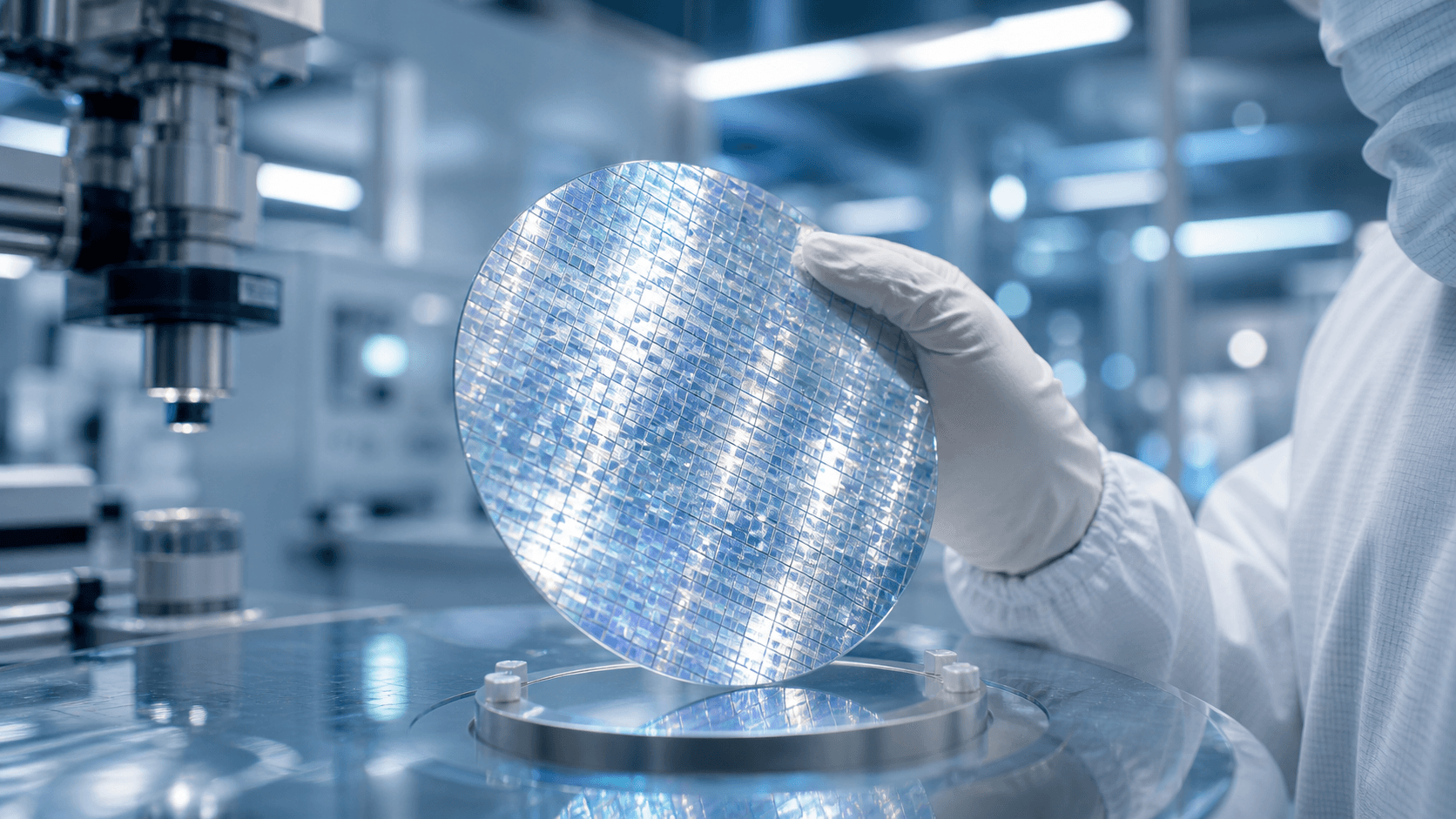
💡Shanghai's material bet could reshape the future hardware pipeline for AI infrastructure.
⚡ 30-Second TL;DR
What Changed
Shanghai began a systematic fourth-generation semiconductor layout in March 2024.
Why It Matters
If the ecosystem matures, these materials could expand the hardware options available for demanding AI and power-electronics workloads. The larger significance is strategic: Shanghai is attempting to convert accumulated research into a domestic semiconductor supply and commercialization pipeline.
What To Do Next
Review your AI hardware roadmap for gallium oxide and diamond power-device suppliers before committing to long-term accelerator or data-center designs.
Key Points
- •Shanghai began a systematic fourth-generation semiconductor layout in March 2024.
- •Lingang is scheduled to advance its first industry cluster construction plan in 2026.
- •Gallium oxide and diamond are identified as the initiative's core materials.
- •Sinan and similar incubators are linking semiconductor research with commercial product development.
🧠 Deep Insight
Background and context from public sources — not the original article. 22 sources cited.
🔑 Enhanced Key Takeaways
- •Shanghai's "fourth-generation semiconductor" initiative in Lingang is formalized by the "Action Plan for Building a Future Industrial Cluster of 4th-Generation Semiconductors (2026–2028)", which is China's first local special industrial policy tailored exclusively to this sector.
- •The Lingang plan defines two major development tracks: ultra-wide bandgap semiconductors, including gallium oxide, diamond, and aluminum nitride, as well as ultra-narrow bandgap semiconductors, such as indium antimonide and gallium antimonide.
- •Gallium oxide is considered a beacon of hope for particularly heat-resistant and cost-effective semiconductors due to its physical properties, enabling higher breakdown voltages and operating temperatures, and can be produced using cost-effective melt growth methods.
- •Sinan Semiconductor incubator, located in the Oriental Chip Port in the Lingang Special Area, offers comprehensive services for semiconductor startups, including EDA design, wafer manufacturing, and packaging and testing certification, and has helped shorten chip design cycles by 30% to 50%.
- •The commercialization of fourth-generation semiconductors, particularly gallium oxide, is projected to have a long timeline, with widespread application potentially arriving after 2040, despite the first device result being reported in 2012.
🛠️ Technical Deep Dive
- Gallium Oxide (Ga2O3):
- An ultra-wide bandgap semiconductor, specifically beta-phase (β-Ga2O3), with a bandgap of 4.7-4.9 eV.
- Exhibits a theoretical breakdown electric field of 8 MV/cm, which is significantly higher than silicon carbide (SiC) and gallium nitride (GaN).
- Possesses a Baliga's Figure of Merit (BFOM) of approximately 3,300, making it fundamentally superior for high-voltage power switching applications compared to SiC and GaN.
- Can be produced using cost-effective melt growth methods like FZ (Floating Zone) and EFG (Edge-defined Film-fed Growth), which allows for larger diameter wafers with fewer crystal faults, unlike SiC or GaN.
- Its thermal conductivity is relatively low, around 0.27 W/cm·K, posing a critical constraint for high-power operation.
- Common device categories include Schottky barrier diodes (SBDs) and field-effect transistors (FETs) in lateral, vertical, and nanomembrane configurations.
- Key challenges include thermal management and achieving effective p-type doping.
- Research indicates that direct integration of CVD-grown diamond layers with Ga2O3 can reduce thermal resistance by up to 60%.
- Diamond (C):
- Known as the ultimate semiconductor material due to its ultra-wide bandgap of 5.47 eV.
- Features high carrier mobility (electron mobility 4000 cm²/V·s, hole mobility 3800 cm²/V·s) and a high critical breakdown electric field of 20 MV/cm.
- Boasts the highest thermal conductivity among semiconductor materials (22 W/cm·K), far superior to SiC and GaN.
- Offers exceptional electrical insulation properties, chemical inertness, stability across extreme temperature ranges, and remarkable mechanical strength.
- Ideal for power devices and applications in harsh environments, such as quantum computing systems, radiation sensors, and communications satellites.
- Challenges include high production costs, limitations in wafer size (currently smaller than 1 inch, though progress towards 4-inch is ongoing), difficulties with deep doping leading to high electrical resistance at room temperature, and complex integration processes.
- The lack of reliable n-type doping limits the development of bipolar devices, with most research focusing on p-type Schottky barrier diodes (SBDs) and unipolar field-effect transistors (FETs).
🔮 Future ImplicationsAI analysis grounded in cited sources
⏳ Timeline
📎 Sources (22)
Factual claims are grounded in the sources below. Forward-looking analysis is AI-generated interpretation.
Weekly AI Recap
Read this week's curated digest of top AI events →
👉Related Updates

AI-curated news aggregator. All content rights belong to original publishers.
Original source: Pandaily ↗
This is a summary, not the original. Read the source, or get the weekly briefing.
Weekly AI briefing
One email a week. Unsubscribe anytime.