Semiconductor TOP10: New Moore's Law Emerges
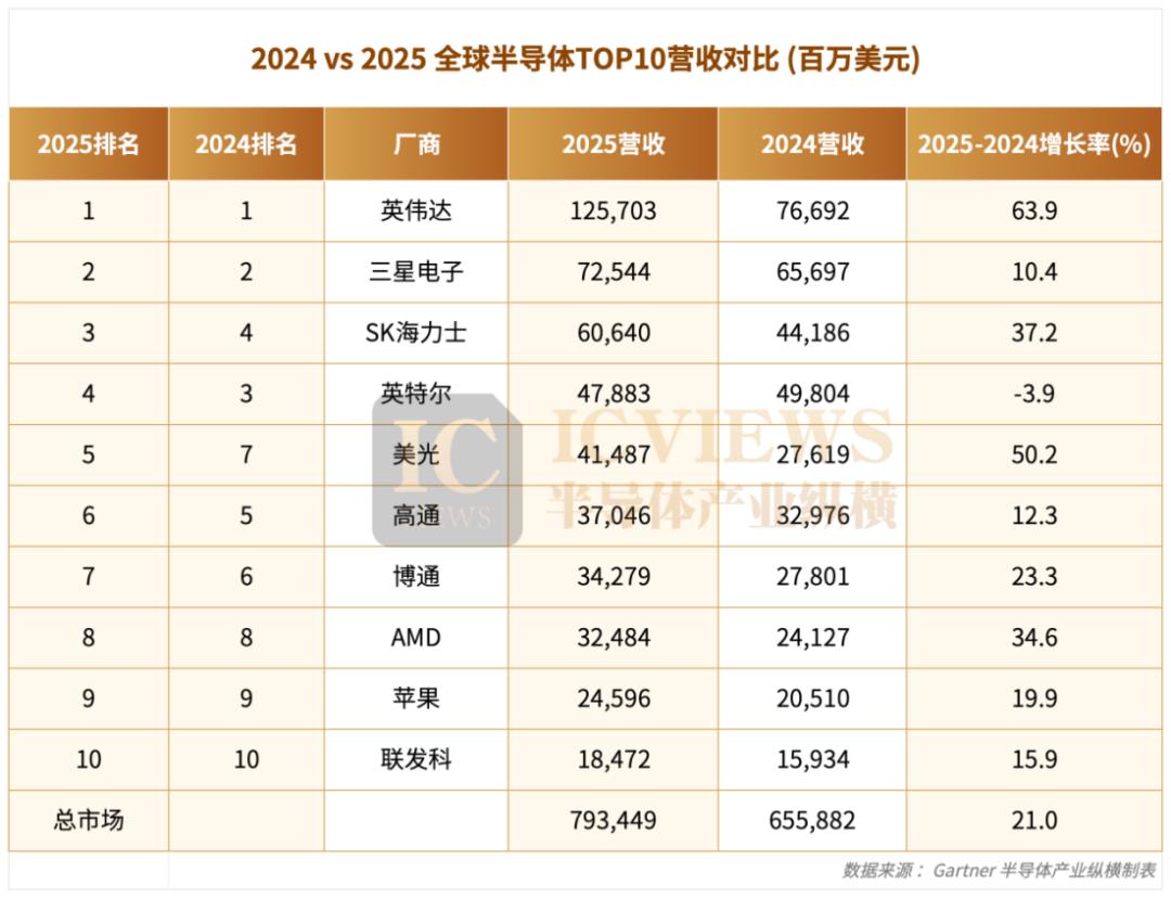
💡$793B semi TOP10 unveils new Moore's Law—shapes AI hardware landscape
⚡ 30-Second TL;DR
What Changed
Global TOP10 semiconductor companies analyzed
Why It Matters
Ranking shifts influence AI chip availability and innovation velocity for practitioners.
What To Do Next
Diversify suppliers by checking latest TOP10 for AI GPU exposure.
Key Points
- •Global TOP10 semiconductor companies analyzed
- •$793 billion market scale
- •Introduction of 'new Moore's Law' driver
🧠 Deep Insight
Background and context from public sources — not the original article. 10 sources cited.
🔑 Enhanced Key Takeaways
- •Traditional Moore's Law is slowing due to physical limits at sub-2nm scales and escalating fabrication costs, including extreme ultraviolet lithography tools doubling every 4 years[1][3][5].
- •Industry is adopting advanced packaging techniques like 3D stacking (e.g., TSMC’s 3DFabric) and heterogeneous integration to boost performance beyond transistor scaling[2][5].
- •TSMC's 2nm process, marking the 'Angstrom Era,' promises 10-15% performance gains and improved power efficiency over 3nm for AI and high-performance computing[2].
- •Innovations such as optical computing and new transistor designs (e.g., FinFET to gate-all-around) are proposed as potential 'new Moore's Law' paradigms for continued scaling[9][8].
🛠️ Technical Deep Dive
- •TSMC’s 2nm process uses gate-all-around (GAA) nanosheet transistors, enabling transistor densities beyond FinFET limits at 3nm[2].
- •3D packaging stacks chips vertically to reduce latency, with TSMC’s 3DFabric integrating logic, memory, and I/O for 20-30% performance uplift without node shrinks[2][5].
- •Extreme ultraviolet lithography (EUV) contributes ~67% to density improvements via optical projection, while optical doping handles the rest[1].
- •Sub-1nm nodes target angstrom-scale gates (e.g., Intel’s roadmap), relying on novel materials to bypass atomic limits[2].
🔮 Future ImplicationsAI analysis grounded in cited sources
⏳ Timeline
📎 Sources (10)
Factual claims are grounded in the sources below. Forward-looking analysis is AI-generated interpretation.
- splunk.com — Moores Law
- patentpc.com — The Future of Moores Law Are We Nearing the Limit Latest Semiconductor Trends
- en.wikipedia.org — Moore's Law
- bench.com — Beyond Moores Law Navigating the Future of Semiconductor Innovation
- csis.org — Advanced Packaging and Future Moores Law
- truthonthemarket.com — The Competitive Chaos Behind Moores Law
- laweconcenter.org — From Moores Law to Market Rivalry the Economic Forces That Shape the Semiconductor Manufacturing Industry
- techxplore.com — 2026 01 Law Famous Road
- allaboutcircuits.com — The New Moores Law Why Optical Computing Could Redefine Scaling for AI
- datacenterknowledge.com — Semiconductor Advancement Is Moore S Law Finally Dead
Weekly AI Recap
Read this week's curated digest of top AI events →
👉Related Updates



AI-curated news aggregator. All content rights belong to original publishers.
Original source: 钛媒体 ↗
This is a summary, not the original. Read the source, or get the weekly briefing.
Weekly AI briefing
One email a week. Unsubscribe anytime.