💰钛媒体•較早收集於 18m
全球半導體TOP10,誰主沉浮
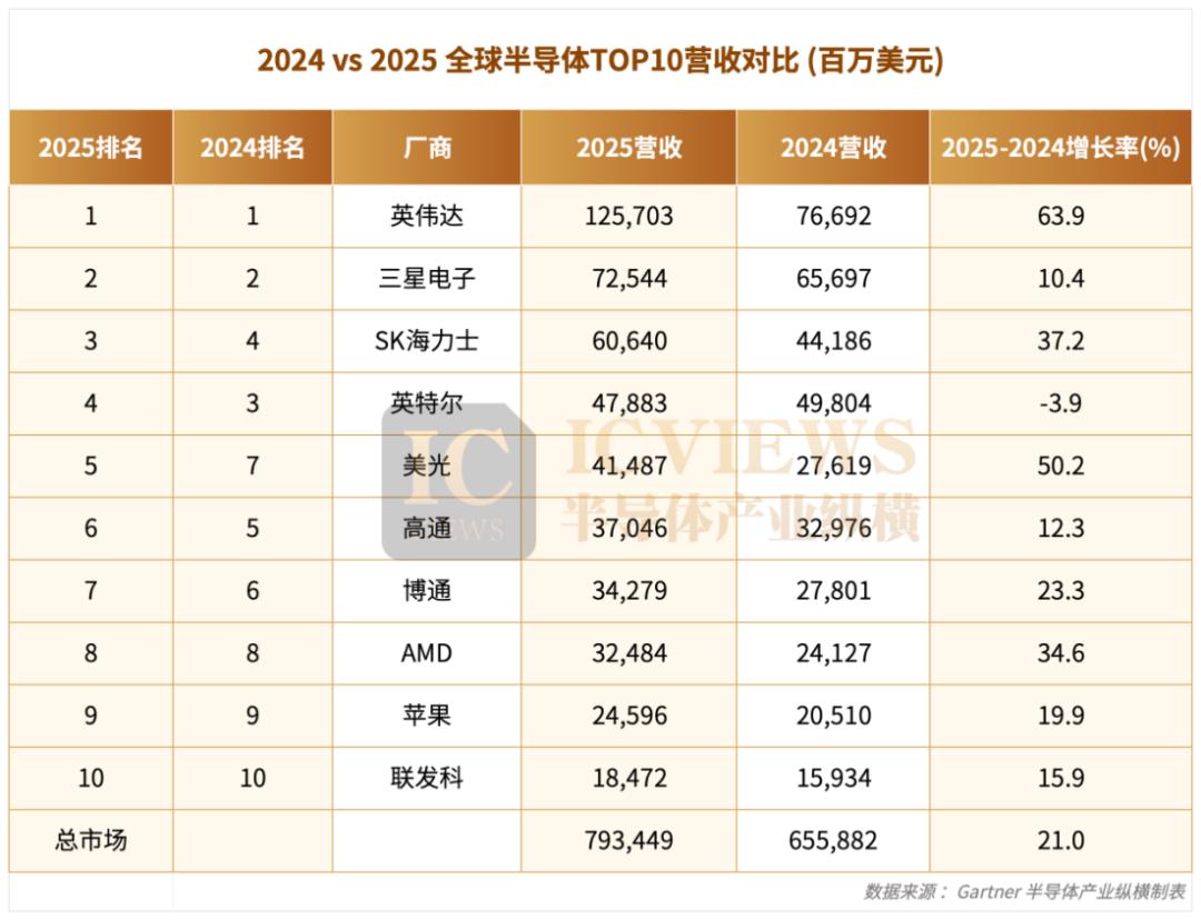
💡$793B semi TOP10 unveils new Moore's Law—shapes AI hardware landscape
⚡ 30-Second TL;DR
有什麼變化
全球半導體TOP10分析
為什麼重要
排名變動影響AI晶片供應與創新速度。
下一步行動
Diversify suppliers by checking latest TOP10 for AI GPU exposure.
誰應關注:Enterprise & Security Teams
關鍵要點
- •全球半導體TOP10分析
- •7930億美元市場規模
- •「新摩爾定律」驅動因素
🧠 深度解析
背景與延伸:來自公開資料,非原文內容。引用 10 個來源。
🔑 增強重點摘要
- •Traditional Moore's Law is slowing due to physical limits at sub-2nm scales and escalating fabrication costs, including extreme ultraviolet lithography tools doubling every 4 years[1][3][5].
- •Industry is adopting advanced packaging techniques like 3D stacking (e.g., TSMC’s 3DFabric) and heterogeneous integration to boost performance beyond transistor scaling[2][5].
- •TSMC's 2nm process, marking the 'Angstrom Era,' promises 10-15% performance gains and improved power efficiency over 3nm for AI and high-performance computing[2].
- •Innovations such as optical computing and new transistor designs (e.g., FinFET to gate-all-around) are proposed as potential 'new Moore's Law' paradigms for continued scaling[9][8].
🛠️ 技術深入
- •TSMC’s 2nm process uses gate-all-around (GAA) nanosheet transistors, enabling transistor densities beyond FinFET limits at 3nm[2].
- •3D packaging stacks chips vertically to reduce latency, with TSMC’s 3DFabric integrating logic, memory, and I/O for 20-30% performance uplift without node shrinks[2][5].
- •Extreme ultraviolet lithography (EUV) contributes ~67% to density improvements via optical projection, while optical doping handles the rest[1].
- •Sub-1nm nodes target angstrom-scale gates (e.g., Intel’s roadmap), relying on novel materials to bypass atomic limits[2].
🔮 前景展望AI analysis grounded in cited sources
Advanced packaging share will reach 35% of wafers by 2026
This growth from 28% in 2020 reflects its role in sustaining performance gains amid transistor scaling limits, supported by U.S. investments like the CHIPS Act[5].
2nm processes will deliver 10-15% speed boost over 3nm
TSMC's Angstrom Era advancements enable higher transistor performance and efficiency, critical for AI and edge computing demands[2].
R&D costs will double every generation through 2030
Moore's second law (Rock's law) documents exponential fab capital increases, straining single-firm dominance and favoring foundry specialization[3].
⏳ 時間線
1965-04
Gordon Moore publishes original observation of transistor doubling every year (later revised to two years)
2012-01
Intel adopts 22nm tri-gate FinFET, departing from planar transistors to sustain scaling
2016-12
ITRS issues final roadmap, shifting from Moore's Law to 'More than Moore' application-driven development
2020-01
Advanced packaging wafers reach 28% market share amid slowing transistor shrinks
2024-12
TSMC announces 2nm process entry into Angstrom Era for sub-nanometer scaling
2025-11
Analysis highlights TSMC displacing Intel via process innovation in competitive semiconductor dynamics
📎 來源 (10)
Factual claims are grounded in the sources below. Forward-looking analysis is AI-generated interpretation.
- splunk.com — Moores Law
- patentpc.com — The Future of Moores Law Are We Nearing the Limit Latest Semiconductor Trends
- en.wikipedia.org — Moore's Law
- bench.com — Beyond Moores Law Navigating the Future of Semiconductor Innovation
- csis.org — Advanced Packaging and Future Moores Law
- truthonthemarket.com — The Competitive Chaos Behind Moores Law
- laweconcenter.org — From Moores Law to Market Rivalry the Economic Forces That Shape the Semiconductor Manufacturing Industry
- techxplore.com — 2026 01 Law Famous Road
- allaboutcircuits.com — The New Moores Law Why Optical Computing Could Redefine Scaling for AI
- datacenterknowledge.com — Semiconductor Advancement Is Moore S Law Finally Dead
📰
AI 週報
閱讀本週精選 AI 大事摘要 →
👉相關動態



AI 策展新聞聚合。所有內容版權歸原始發布者所有。
原始來源: 钛媒体 ↗
每週 AI 簡報
每週一封,可隨時退訂。