Samsung Unveils Three Memory Designs for AI Data Centers
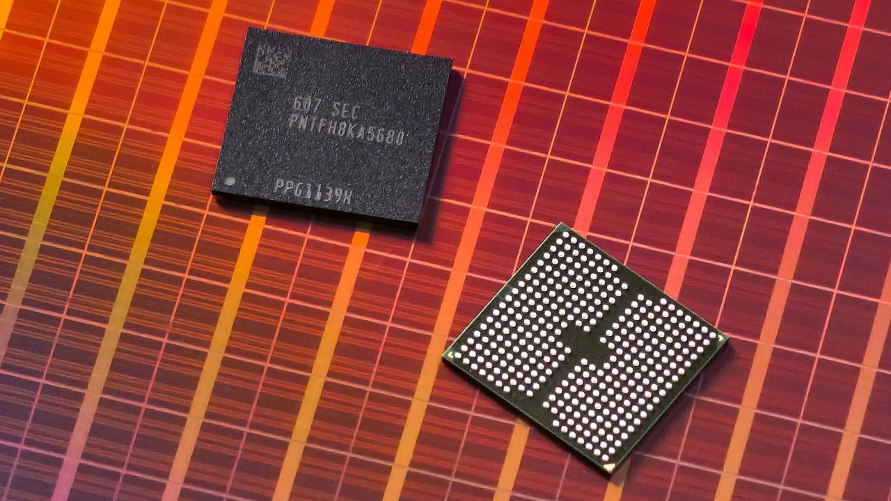
Samsung’s three bonded-memory designs could shape the next generation of AI data-center hardware.
30-Second TL;DR
What Changed
Samsung introduced zHBM, zNAND-O, and BV-NAND at FMS.
Why It Matters
More specialized memory options could help AI infrastructure providers optimize bandwidth, capacity, and storage for different workloads. Samsung’s approach also highlights wafer bonding as an important technology for scaling next-generation AI memory.
What To Do Next
Track Samsung’s forthcoming specifications for zHBM, zNAND-O, and BV-NAND before planning your next AI server memory refresh.
Key Points
- •Samsung introduced zHBM, zNAND-O, and BV-NAND at FMS.
- •The three technologies address different AI data-center memory requirements.
- •Advanced wafer bonding is the common manufacturing approach across the designs.
Deep Insight
AI-generated analysis for this event — not the original article.
Enhanced Key Takeaways
- •zHBM utilizes a specialized logic die with integrated processing capabilities, moving beyond traditional passive memory to support near-memory computing for AI inference.
- •zNAND-O is designed specifically for high-capacity AI training datasets, implementing a new interface protocol that reduces latency during random read operations by up to 30% compared to standard NAND.
- •BV-NAND (Bonded Vertical NAND) leverages a wafer-to-wafer bonding process that allows for higher cell density and improved thermal dissipation, addressing the heat constraints of dense AI server racks.
- •The common wafer-bonding architecture across these products is part of Samsung's 'Advanced Packaging' strategy to combat the memory wall by shortening interconnect distances between compute and storage.
- •Samsung is positioning these technologies to integrate directly into CXL (Compute Express Link) 3.0/4.0 ecosystems, enabling disaggregated memory pools for large-scale AI clusters.
Competitor Analysis
- Samsung (zHBM/zNAND)
- Wafer-Bonded Logic/NAND
- SK Hynix (HBM3E/4)
- TSV-based Stacked DRAM
- Micron (HBM3 Gen2/4)
- TSV-based Stacked DRAM
- Samsung (zHBM/zNAND)
- Near-Memory/Storage AI
- SK Hynix (HBM3E/4)
- High-Bandwidth Training
- Micron (HBM3 Gen2/4)
- High-Bandwidth Training
- Samsung (zHBM/zNAND)
- Native CXL 3.0+ Support
- SK Hynix (HBM3E/4)
- Emerging CXL Support
- Micron (HBM3 Gen2/4)
- Emerging CXL Support
| Feature | Samsung (zHBM/zNAND) | SK Hynix (HBM3E/4) | Micron (HBM3 Gen2/4) |
|---|---|---|---|
| Architecture | Wafer-Bonded Logic/NAND | TSV-based Stacked DRAM | TSV-based Stacked DRAM |
| Primary Focus | Near-Memory/Storage AI | High-Bandwidth Training | High-Bandwidth Training |
| CXL Integration | Native CXL 3.0+ Support | Emerging CXL Support | Emerging CXL Support |
Technical Deep Dive
- zHBM: Incorporates a programmable logic layer within the HBM stack to handle data filtering and pre-processing, reducing the load on the primary GPU/NPU.
- zNAND-O: Features a multi-plane architecture that allows for parallel data access, specifically optimized for the small-block random reads typical of Large Language Model (LLM) inference.
- BV-NAND: Utilizes hybrid bonding (Cu-to-Cu) to eliminate traditional micro-bumps, significantly increasing I/O density and reducing power consumption per bit transferred.
- Interconnects: All three designs utilize a unified 3D-IC packaging platform that supports high-speed signaling protocols designed to minimize signal integrity degradation at high frequencies.
Future ImplicationsAI analysis grounded in cited sources
Timeline
- 2023-10Samsung announces expansion of its Advanced Packaging (AVP) business unit to focus on HBM and 3D-IC.
- 2024-05Samsung reveals roadmap for CXL-based memory expansion modules at the Samsung AI Forum.
- 2025-02Samsung achieves mass production milestone for 12-layer HBM3E using advanced thermal compression bonding.
- 2026-08Samsung unveils zHBM, zNAND-O, and BV-NAND at FMS, marking the transition to wafer-bonded AI memory.
Weekly AI Recap
Read this week's curated digest of top AI events →
AI-curated news aggregator. All content rights belong to original publishers.
Original source: Tom's Hardware ↗
This is a summary, not the original. Read the source, or get the weekly briefing.
The weekly digest
One email a week. Unsubscribe anytime.