來源Tom's Hardware•較早收集於 13m
Samsung 推出三款 AI 資料中心記憶體設計
#wafer-bonding#ai-memory#data-center-hardwaresamsung-zhbm,-znand-o,-and-bv-nandsamsungzhbmznand-obv-nand
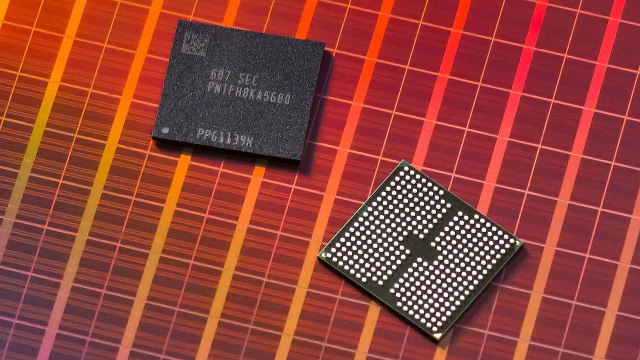
Samsung 的三款鍵合記憶體設計可能影響下一代 AI 資料中心硬體。
30 秒速覽
有什麼變化
Samsung 在 FMS 發表 zHBM、zNAND-O 與 BV-NAND。
為什麼重要
更多專用記憶體選項可能協助 AI 基礎設施業者針對不同工作負載最佳化頻寬、容量與儲存。Samsung 的方案也凸顯晶圓鍵合是擴展下一代 AI 記憶體的重要技術。
下一步行動
在規劃下一次 AI 伺服器記憶體升級前,持續追蹤 Samsung 即將公布的 zHBM、zNAND-O 與 BV-NAND 規格。
誰應關注:Enterprise & Security Teams
關鍵要點
- •Samsung 在 FMS 發表 zHBM、zNAND-O 與 BV-NAND。
- •三項技術分別滿足 AI 資料中心的不同記憶體需求。
- •先進晶圓鍵合是這些設計共同採用的製造方式。
深度解析
本篇為 AI 生成分析,非原文內容。
增強重點摘要
- •zHBM utilizes a specialized logic die with integrated processing capabilities, moving beyond traditional passive memory to support near-memory computing for AI inference.
- •zNAND-O is designed specifically for high-capacity AI training datasets, implementing a new interface protocol that reduces latency during random read operations by up to 30% compared to standard NAND.
- •BV-NAND (Bonded Vertical NAND) leverages a wafer-to-wafer bonding process that allows for higher cell density and improved thermal dissipation, addressing the heat constraints of dense AI server racks.
- •The common wafer-bonding architecture across these products is part of Samsung's 'Advanced Packaging' strategy to combat the memory wall by shortening interconnect distances between compute and storage.
- •Samsung is positioning these technologies to integrate directly into CXL (Compute Express Link) 3.0/4.0 ecosystems, enabling disaggregated memory pools for large-scale AI clusters.
競品分析
Architecture
- Samsung (zHBM/zNAND)
- Wafer-Bonded Logic/NAND
- SK Hynix (HBM3E/4)
- TSV-based Stacked DRAM
- Micron (HBM3 Gen2/4)
- TSV-based Stacked DRAM
Primary Focus
- Samsung (zHBM/zNAND)
- Near-Memory/Storage AI
- SK Hynix (HBM3E/4)
- High-Bandwidth Training
- Micron (HBM3 Gen2/4)
- High-Bandwidth Training
CXL Integration
- Samsung (zHBM/zNAND)
- Native CXL 3.0+ Support
- SK Hynix (HBM3E/4)
- Emerging CXL Support
- Micron (HBM3 Gen2/4)
- Emerging CXL Support
| Feature | Samsung (zHBM/zNAND) | SK Hynix (HBM3E/4) | Micron (HBM3 Gen2/4) |
|---|---|---|---|
| Architecture | Wafer-Bonded Logic/NAND | TSV-based Stacked DRAM | TSV-based Stacked DRAM |
| Primary Focus | Near-Memory/Storage AI | High-Bandwidth Training | High-Bandwidth Training |
| CXL Integration | Native CXL 3.0+ Support | Emerging CXL Support | Emerging CXL Support |
技術深入
- zHBM: Incorporates a programmable logic layer within the HBM stack to handle data filtering and pre-processing, reducing the load on the primary GPU/NPU.
- zNAND-O: Features a multi-plane architecture that allows for parallel data access, specifically optimized for the small-block random reads typical of Large Language Model (LLM) inference.
- BV-NAND: Utilizes hybrid bonding (Cu-to-Cu) to eliminate traditional micro-bumps, significantly increasing I/O density and reducing power consumption per bit transferred.
- Interconnects: All three designs utilize a unified 3D-IC packaging platform that supports high-speed signaling protocols designed to minimize signal integrity degradation at high frequencies.
前景展望基於引用來源的 AI 分析
Samsung will shift its primary NAND revenue focus from consumer SSDs to AI-specific zNAND-O products by 2027.
The specialized architecture of zNAND-O provides higher margins and addresses the growing bottleneck of data ingestion in AI training clusters.
The adoption of wafer-bonding for memory will become the industry standard for all HBM4 and beyond designs.
Thermal and density limitations of traditional TSV-only stacking are forcing manufacturers to adopt advanced bonding techniques to maintain performance scaling.
時間線
2023-10
Samsung announces expansion of its Advanced Packaging (AVP) business unit to focus on HBM and 3D-IC.
2024-05
Samsung reveals roadmap for CXL-based memory expansion modules at the Samsung AI Forum.
2025-02
Samsung achieves mass production milestone for 12-layer HBM3E using advanced thermal compression bonding.
2026-08
Samsung unveils zHBM, zNAND-O, and BV-NAND at FMS, marking the transition to wafer-bonded AI memory.
- 2023-10Samsung announces expansion of its Advanced Packaging (AVP) business unit to focus on HBM and 3D-IC.
- 2024-05Samsung reveals roadmap for CXL-based memory expansion modules at the Samsung AI Forum.
- 2025-02Samsung achieves mass production milestone for 12-layer HBM3E using advanced thermal compression bonding.
- 2026-08Samsung unveils zHBM, zNAND-O, and BV-NAND at FMS, marking the transition to wafer-bonded AI memory.
AI 週報
閱讀本週精選 AI 大事摘要 →
AI 策展新聞聚合。所有內容版權歸原始發布者所有。
原始來源: Tom's Hardware ↗
每週電子報
每週一封,可隨時退訂。